Supercharge Your Innovation With Domain-Expert AI Agents!

A pixel driving circuit and a compensation method of the pixel driving circuit

A technology of pixel drive circuit and compensation module, applied in instruments, static indicators, etc., can solve problems such as threshold voltage drift, different display images, afterimage, etc., and achieve the effect of improving luminous uniformity and image quality

Active Publication Date: 2019-06-25
SHENZHEN CHINA STAR OPTOELECTRONICS SEMICON DISPLAY TECH CO LTD
View PDF16 Cites 10 Cited by
  • Summary
  • Abstract
  • Description
  • Claims
  • Application Information

AI Technical Summary

Problems solved by technology

Although oxide thin film transistors have better process uniformity, similar to amorphous silicon thin film transistors, their threshold voltage will drift under long-term pressure and high temperature, resulting in different display screens. Different threshold shifts will cause differences in display brightness
This difference is related to the previously displayed image, so it often appears as an afterimage phenomenon

Method used


Image

  • A pixel driving circuit and a compensation method of the pixel driving circuit
  • A pixel driving circuit and a compensation method of the pixel driving circuit
  • A pixel driving circuit and a compensation method of the pixel driving circuit

Examples


Embodiment Construction

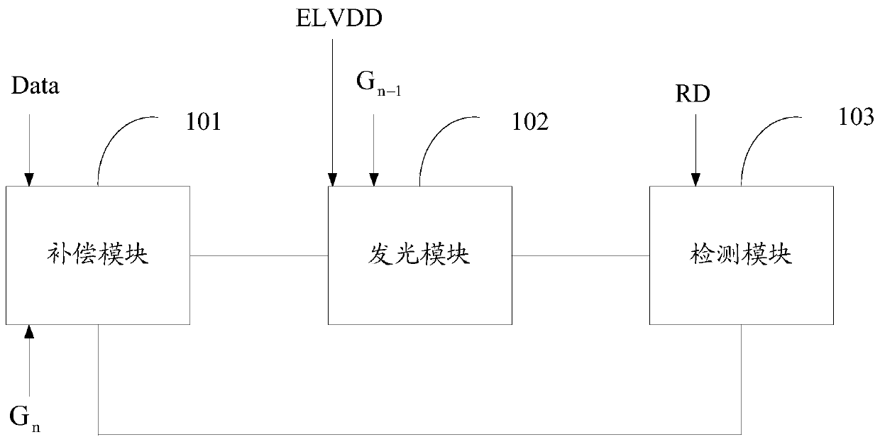
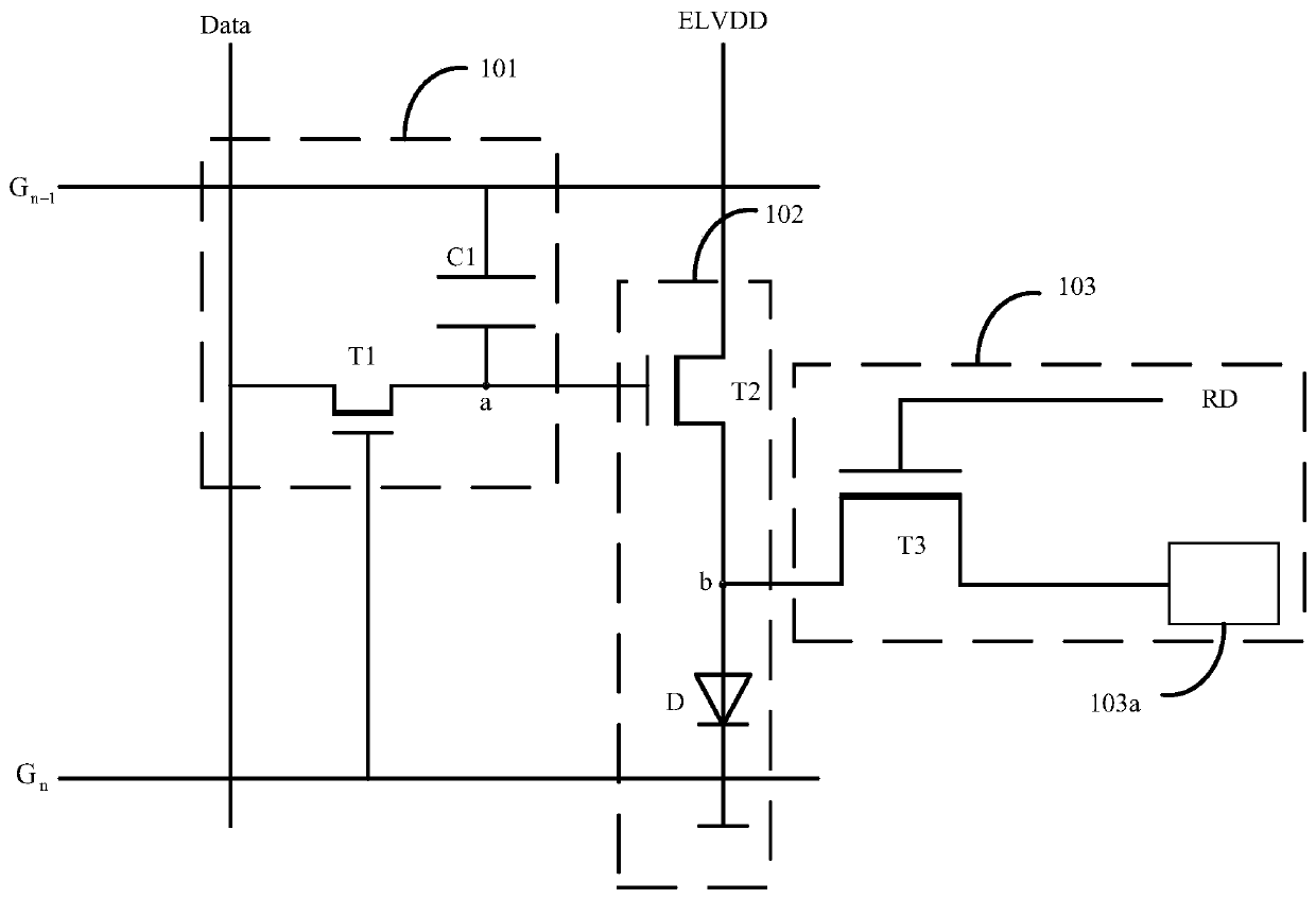
[0035] The technical solutions in the embodiments of the present application will be clearly and completely described below in conjunction with the drawings in the embodiments of the present application. Apparently, the described embodiments are only some of the embodiments of this application, not all of them. Based on the embodiments in this application, all other embodiments obtained by those skilled in the art without making creative efforts belong to the scope of protection of this application.

[0036] The transistors used in all embodiments of this application can be thin film transistors or field effect transistors or other devices with the same characteristics. Since the source and drain of the transistors used here are symmetrical, their source and drain can be interchanged. of. In the embodiment of the present application, in order to distinguish the two poles of the transistor except the gate, one pole is called the source, and the other pole is called the drain. ...


PUM


Abstract

The invention provides a pixel driving circuit and a compensation method of the pixel driving circuit. A pixel driving circuit with a 3T1C structure is adopted. The actual current of the driving transistor in each pixel is detected, and the threshold voltage of the driving transistor in each pixel is determined according to the actual current, so that the driving transistor in each pixel is effectively compensated, the purpose of improving the light emitting uniformity of the light emitting device is achieved, and the image quality is improved.

Description

technical field [0001] The present application relates to the field of display technology, in particular to a pixel driving circuit and a compensation method for the pixel driving circuit. Background technique [0002] In the prior art, the transistors in the pixel driving circuit are mostly low-temperature polysilicon thin film transistors or oxide thin film transistors. Compared with general amorphous silicon thin film transistors, low-temperature polysilicon thin film transistors and oxide thin film transistors have higher mobility and more stable characteristics, and are more suitable for active-matrix organic light-emitting diodes (Active-matrix organic light-emitting diodes). diode, AMOLED) display. [0003] However, due to the limitations of the crystallization process, low-temperature polysilicon thin film transistors fabricated on large-area glass substrates often have non-uniformity in electrical parameters such as threshold voltage and mobility. This non-uniform...

Claims


Application Information

Patent Timeline
Patent Type & Authority Applications(China)
IPC IPC(8): G09G3/3225
CPCG09G3/32G09G3/3225
Inventor 李新吉
Owner SHENZHEN CHINA STAR OPTOELECTRONICS SEMICON DISPLAY TECH CO LTD
Features
  • R&D
  • Intellectual Property
  • Life Sciences
  • Materials
  • Tech Scout
  • Unparalleled Data Quality
  • Higher Quality Content
  • 60% Fewer Hallucinations
Learn More