Display panel film layer structure and preparation process thereof

A technology of film layer structure and display panel, which is applied in the directions of instruments, computing, and electrical digital data processing, etc., can solve the problems of high reflection in the visual area of ​​the touch screen and affect the display effect of the panel, and achieve simple and compact structure, low process cost, and solution The effect of poor adhesion

Active Publication Date: 2019-07-09
GUANGZHOU GOVISIONOX TECH CO LTD
View PDF18 Cites 1 Cited by
  • Summary
  • Abstract
  • Description
  • Claims
  • Application Information

AI Technical Summary

Problems solved by technology

The touch screen of the above traditional design has interface reflection between different media interfaces, resulting in high reflection in the visible area of ​​the touch screen, which seriously affects the display effect of the panel

Method used


Image

  • Display panel film layer structure and preparation process thereof
  • Display panel film layer structure and preparation process thereof
  • Display panel film layer structure and preparation process thereof

Examples


Embodiment Construction

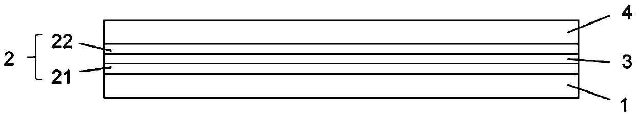
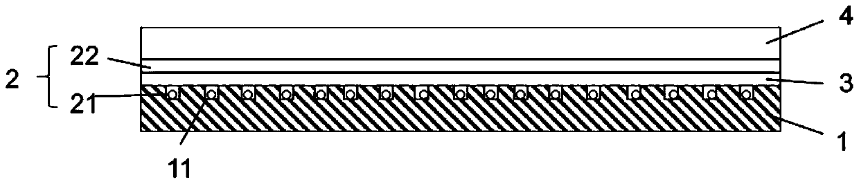
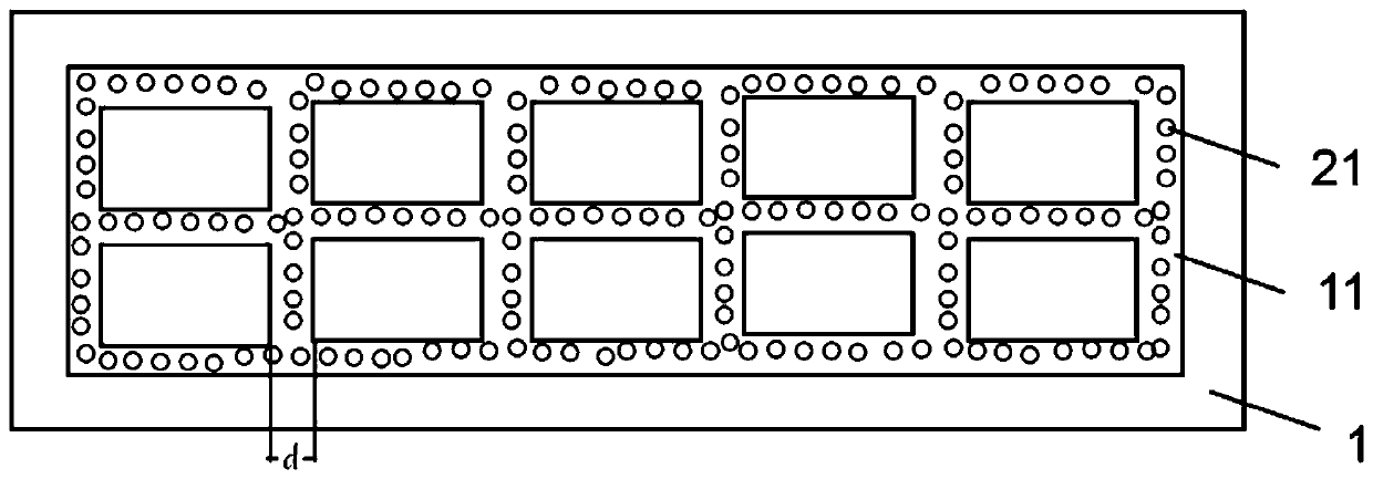
[0035] In order to make the purpose, technical solution and advantages of the present application clearer, the following will clearly and completely describe the technical solution of the present application in combination with specific implementation methods of the present application and corresponding drawings. Apparently, the described implementations are only some of the implementations of this application, not all of them. Based on the implementation manners in this application, all other implementation manners obtained by persons of ordinary skill in the art without making creative efforts belong to the scope of protection of this application.

[0036] Embodiments of the present invention are described in detail below, examples of which are shown in the drawings, wherein the same or similar reference numerals denote the same or similar elements or elements having the same or similar functions throughout. The embodiments described below by referring to the figures are exe...


PUM

PropertyMeasurementUnit
widthaaaaaaaaaa
widthaaaaaaaaaa
diameteraaaaaaaaaa

Abstract

The invention relates to a display panel film layer structure. The display panel film layer structure comprises a substrate, a conductive film layer, an optical adhesive film layer and a cover body, wherein the substrate, the conductive film layer, the optical adhesive film layer and the cover body are stacked; the conductive film layer comprises a first electrode and a second electrode which aresequentially arranged from bottom to top; the optical adhesive film layer is arranged between the first electrode and the second electrode; and the substrate is provided with a substrate channel for accommodating the first electrode. Metal nano-particles are deposited in a grid channel formed by etching a TFE upper-layer film through atomic layer deposition to form macroscopic metal nanowires, sothat the adhesion between the metal nanowires and the substrate is improved, and meanwhile, the haze problem of a display device can be improved.

Description

technical field [0001] The invention relates to the field of display technology, in particular to a film layer structure of a display panel and a preparation process thereof. Background technique [0002] Touch screen, also known as touch panel, is an inductive liquid crystal display device used to receive input signals such as contacts. When a certain area on the screen is touched, its tactile feedback system can drive various electronic devices according to pre-programmed programs. And through the liquid crystal display screen to create a vivid audio-visual effects. At present, touch screens are widely used in various electronic devices, and smart phones account for a large proportion. Smartphone touch screens can be divided into resistive screens and capacitive screens. The capacitive touch screen is a layer of transparent special metal conductive material on the glass surface. When the finger touches the metal layer, the capacitance of the contact will change, so that ...

Claims


Application Information

Patent Timeline
Patent Type & Authority Applications(China)
IPC IPC(8): G02F1/1333G06F3/041
CPCG02F1/13338G06F3/0412
Inventor 张久杰罗志忠丁德宝高建朱娜娜
Owner GUANGZHOU GOVISIONOX TECH CO LTD
Why Eureka
Try Eureka