Display panel and preparation method of display panel

A display panel and substrate technology, applied in nonlinear optics, instruments, optics, etc., can solve problems affecting product electrical properties and yield, peeling, complexity, etc., and achieve the effects of improving electrical properties and yield and reducing stress

Inactive Publication Date: 2019-07-09
TCL CHINA STAR OPTOELECTRONICS TECH CO LTD
View PDF2 Cites 4 Cited by
  • Summary
  • Abstract
  • Description
  • Claims
  • Application Information

AI Technical Summary

Problems solved by technology

However, in the existing display panel, as a planarization layer, before forming PFA, it will face various complex terrains of different bottom layers, such as the stacking of metal layers in the lower layers, especially for thicker metal films. Technology products lead to more complex terrain before forming PFA, and at the same time, it is necessary to open holes in this complex terrain, so that after PFA film formation, at the edge of the module metal line width, due to the effect of stress As a result, the PFA layer is peeled off here, which affects the electrical properties and yield of the product.
[0004] To sum up, the existing display panels have the problem that the planarization layer in the display panel is peeled off due to stress at the edge of the metal line width, which affects the electrical properties and yield of the product.

Method used


Image

  • Display panel and preparation method of display panel
  • Display panel and preparation method of display panel
  • Display panel and preparation method of display panel

Examples


Embodiment Construction

[0032] The technical solutions in the embodiments of the disclosure will be clearly and completely described below in conjunction with the drawings in the embodiments of the disclosure. Apparently, the described embodiments are only some of the embodiments of the present disclosure, not all of them. Based on the embodiments in the present disclosure, all other embodiments obtained by those skilled in the art without creative efforts fall within the protection scope of the present disclosure.

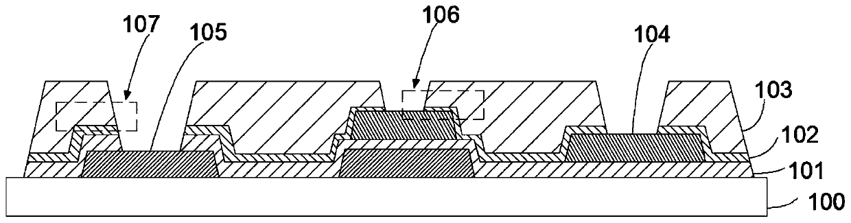
[0033] With the development of LCD display panels in the direction of large size and high resolution, a transparent organic insulating flat layer will be used inside the panel during design to prevent mutual interference of internal electric fields. However, as a flattening layer, it needs to face various complex underlying terrains. Specifically, such as figure 1 as shown in figure 1 It is a schematic diagram of the structure of each layer of the display panel in the existing product...


PUM


Abstract

The invention provides a display panel and a preparation method of the display panel. The display panel comprises a substrate, a device layer on the substrate and a flat layer on the device layer; thedisplay panel further comprises a color resistance layer; and the color resistance layer is arranged between the device layer and the flat layer. Through extending the color resistance layer in a display area to a surrounding gate driving area, the terrain is more flat when the color resistance layer is arranged on the flat layer, so that the stress problems at the wide edges of metal wires are reduced and the condition of flat layer stripping is avoided.

Description

technical field [0001] The present disclosure relates to the field of display technology, and in particular to a display panel and a method for manufacturing the display panel. Background technique [0002] Liquid Crystal Display (LCD) has many advantages such as thin body, power saving, and no radiation, and is widely used in LCD TVs, mobile phones, computer screens and other fields. [0003] Most of the liquid crystal displays currently on the market are backlight liquid crystal displays, which include a liquid crystal display panel and a backlight module. With the gradual development of LCD in the direction of large size, high resolution, high color saturation, etc., large-size LCD panels are also more inclined to use a layer of transparent organic insulating flat layer (Polymer Film On Array, PFA) to prevent mold The mutual interference between the electric fields in the group can effectively improve the display color difference caused by terrain factors, reduce the par...

Claims


Application Information

Patent Timeline
IPC IPC(8): G02F1/1362G02F1/1335G02F1/1333G02F1/1368
CPCG02F1/1333G02F1/133514G02F1/1362G02F1/1368G02F1/136222
Inventor 于承忠
Owner TCL CHINA STAR OPTOELECTRONICS TECH CO LTD
Why Eureka
Try Eureka