Buffer interface circuit and method and application for transmitting data based on circuit

A technology of interface circuit and buffer, which is applied in the field of buffer interface circuit, can solve the problem of low buffer access efficiency and achieve the effect of realizing, improving data interaction efficiency, and high-efficiency data interaction

Active Publication Date: 2019-07-12
XIAN MICROELECTRONICS TECH INST
View PDF8 Cites 2 Cited by
  • Summary
  • Abstract
  • Description
  • Claims
  • Application Information

AI Technical Summary

Problems solved by technology

[0005] The present invention aims at the high-performance SoC / MCU system multi-level bus structure to high-speed peripheral multi-level access requirements, and at the same time for the situation that the buffer access efficiency is not high under the traditional time-sharing access strategy, proposes a buffer interface circuit and based on the circuit The method and application of data transmission realizes high-efficiency data interaction between on-chip multi-level buses and peripherals, improves performance and efficiency under the premise of ensuring correct and reliable transmission, and effectively solves the problem of current ultra-large-scale complex chips such as SoC. , MCU and other internal multi-level bus hosts and the problem of high-efficiency data transmission between peripheral interfaces

Method used


Image

  • Buffer interface circuit and method and application for transmitting data based on circuit
  • Buffer interface circuit and method and application for transmitting data based on circuit
  • Buffer interface circuit and method and application for transmitting data based on circuit

Examples


Embodiment Construction

[0050] The present invention will be further described in detail below in conjunction with specific embodiments, which are explanations of the present invention rather than limitations.

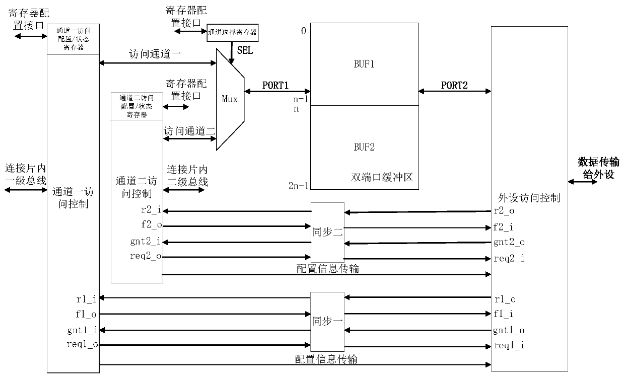
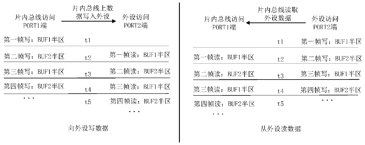
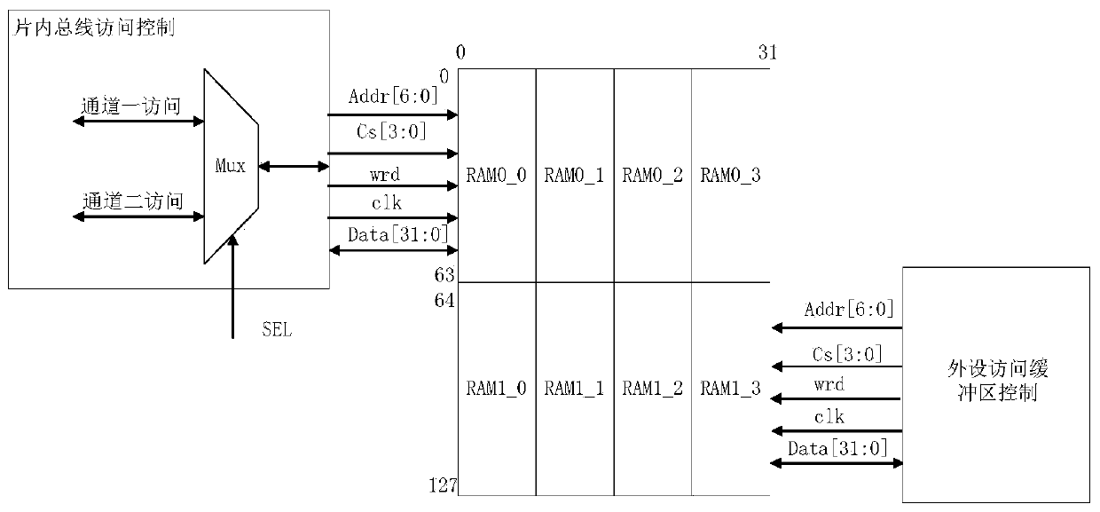
[0051] Such as figure 1 As shown, the buffer interface circuit of the present invention is a high-speed buffer interface circuit based on two-stage pipeline control across multiple clock domains, including a channel-one access control module, a channel-two access control module, a MUX unit, and a synchronization module , Synchronous second module, dual-port buffer and peripheral access buffer control module.

[0052] One end of the channel-one access control module is connected to the on-chip first-level bus, and the other end is connected to the dual-port buffer after being selected by the MUX unit. At the same time, the channel-one access control module exchanges control information with the peripheral access buffer control module by synchronizing the first module. One end of the channel t...


PUM


Abstract

The invention provides a buffer interface circuit, comprising a first channel access control module, a second channel access control module, a channel selection register, an MUX unit, a first synchronous module, a second synchronous module, a dual-port buffer area and a peripheral access buffer area control module. One ends of the first channel access control module and the second channel access control module are correspondingly connected with the on-chip primary bus and the on-chip secondary bus respectively, and the other ends of the first channel access control module and the second channel access control module are connected with the dual-port buffer area after being selected by the MUX unit. The first channel access control module and the second channel access control module respectively carry out control information interaction with the peripheral access buffer area control module through the first synchronous module and the second synchronous module. One end of the peripheral access buffer area control module is connected with the dual-port buffer area, and the other end is connected with the peripheral module. High-efficiency data interaction between the on-chip multi-stage bus and the peripheral is achieved. Performance and efficiency are improved on the premise that correct and reliable transmission is guaranteed, and the problem of high-efficiency data transmissionbetween an internal multi-stage bus host and a peripheral interface is effectively solved.

Description

technical field [0001] The invention belongs to the field of integrated circuit design, and relates to a buffer interface circuit and a data transmission method and application based on the circuit. Background technique [0002] In large-scale complex chips with multiple clock domains, the performance of interface circuits usually determines the data access bandwidth and system operating efficiency. Designing a high-speed interface circuit that takes into account speed, flexibility, reliability and ease of use is often the key point of chip design. [0003] The traditional buffer interface circuit is usually implemented based on fifo structure or dual-port ram structure combined with hardware control circuit. The control strategy and implementation of the hardware control circuit determine the transmission efficiency and performance of the interface buffer circuit. The traditional design usually adopts a time-sharing access strategy. The control circuits of the two clock d...

Claims


Application Information

Patent Timeline
Patent Type & Authority Applications(China)
IPC IPC(8): G06F13/40
CPCG06F13/4022
Inventor 罗敏涛娄冕崔媛媛李磊
Owner XIAN MICROELECTRONICS TECH INST
Why Eureka
Try Eureka