How nldmos is made

A manufacturing method and body region technology, applied in the direction of semiconductor/solid-state device manufacturing, semiconductor devices, electrical components, etc., can solve the problems of SLDMOS failure and inability to form a channel, and achieve the effect of preventing channel failure and device failure.

Active Publication Date: 2021-06-08
SHANGHAI HUAHONG GRACE SEMICON MFG CORP
View PDF0 Cites 0 Cited by
  • Summary
  • Abstract
  • Description
  • Claims
  • Application Information

AI Technical Summary

Problems solved by technology

exist Figure 2A In the corresponding ion implantation 203 of the P-type body region 109, during the process of etching the polysilicon layer 111 to form the first side of the polysilicon gate 111, a polymer (polymer) will be generated and the polymer will adhere On the surface of the photoresist pattern 201, this will make it impossible for the ion implantation 203 in some regions to implant impurities into the inside of the first side surface of the polysilicon gate 111 along the width direction of the channel, so that the formation of the The channel, that is, the channel must be formed by inversion of the surface of the covered P-type body region 109 through the polysilicon gate 111, and the ion implantation 203 cannot implant impurities into the first layer of the polysilicon gate 111. When the side is inside, the channel cannot be formed, which will lead to SLDMOS failure

Method used


Image

  • How nldmos is made
  • How nldmos is made
  • How nldmos is made

Examples


Embodiment Construction

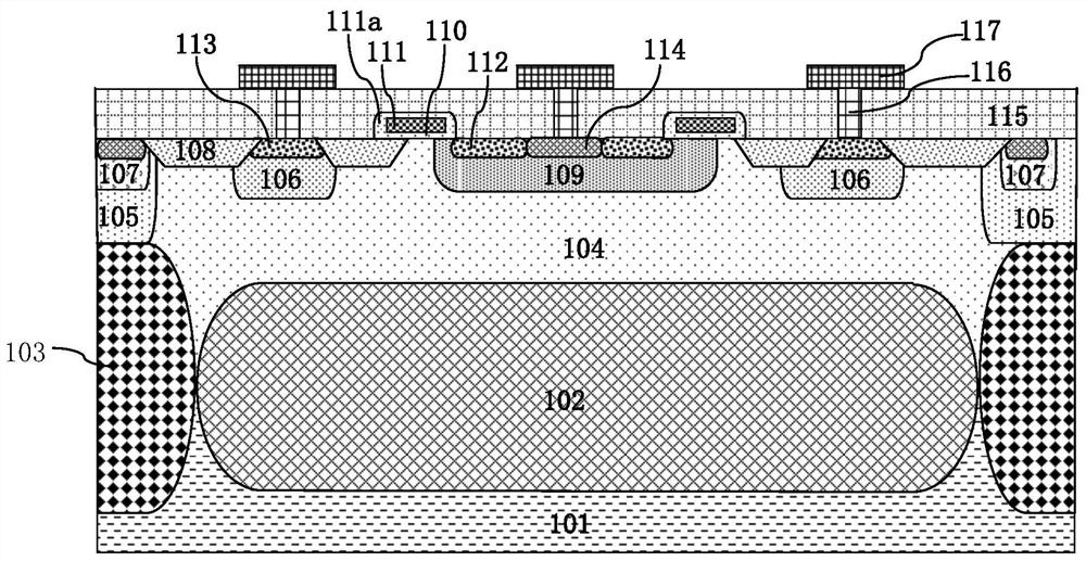
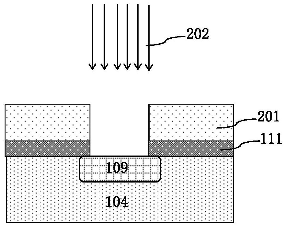
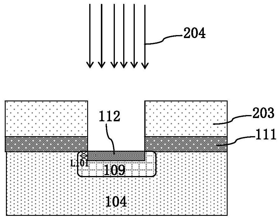
[0058] Such as image 3 Shown is the flow chart of the method of the embodiment of the present invention; Figure 4A to Figure 4D As shown, it is a device structure diagram in the step of forming the P-type body region 109 in the method of the embodiment of the present invention. In the manufacturing method of NLDMOS in the embodiment of the present invention:

[0059] In the manufacturing method of the NLDMOS of the embodiment of the present invention:

[0060] First, form a deep N well 104, a low voltage N well 106, a field oxygen isolation layer 108 on the semiconductor substrate such as a silicon substrate 101, and deposit a gate dielectric layer such as a gate oxide layer 110 and The polysilicon gate 111 specifically includes: after forming an N-type buried layer 102 and a P-type buried layer 103 on the silicon substrate 101, a deep N well 104 is defined, and the deep N well 104 is formed by N-type implantation and annealing. After that, the field oxygen isolation layer...


PUM


Abstract

The invention discloses a manufacturing method of NLDMOS. The body region forming step includes: forming a first photoresist pattern with a first opening defining a P-type body region. Etching is performed to expose the surface of the deep N well, and the first side of the polysilicon gate formed after etching has a second opening. Perform ashing treatment on the first photoresist pattern; the ashing treatment removes the surface part of the first photoresist pattern formed with polymer on the surface and expands the first opening into a third opening, and the second and third openings A polysilicon protruding portion composed of the first polysilicon layer is formed between them. Ion implantation of the P-type body region is performed. Rapid thermal annealing is performed after removing the first photoresist pattern. The gate structure is formed by photolithography. A spacer is formed on a side of the gate structure. N-type heavily doped source and drain implants are performed to form source and drain regions. The invention can eliminate the bad effect of the polymer in the implantation of the P-type body region, so that a good channel can be formed and the length of the channel can be well controlled.

Description

technical field [0001] The invention relates to a semiconductor integrated circuit manufacturing process method, in particular to a NLDMOS manufacturing method. Background technique [0002] The process of simultaneously bipolar junction transistor (BJT), CMOS device and DMOS device on the same chip is a BCD process, such as figure 1 As shown, it is a schematic structural diagram of a switch type (Switch) NLDMOS in the existing BCD process, that is, an N-type LDMOS (laterally diffused metal oxide semiconductor). The switch type NLDMOS is usually also referred to as SNLDMOS for short; NLDMOS mainly includes: An N-type buried layer (NBL) 102, a P-type buried layer (PBL) 103, and a deep N well (DNW) 104 are formed on it; a high-voltage P-well (HVPW) 105 is formed on the top of the P-type buried layer 103, and a high-voltage P-well (HVPW) 105 is formed in the high-voltage P-well 105 There is a low-voltage P well (LVPW) 107, a P+ region is formed on the top surface of the low-vo...

Claims


Application Information

Patent Timeline
Patent Type & Authority Patents(China)
IPC IPC(8): H01L29/78H01L29/06H01L21/336
CPCH01L29/0603H01L29/66681H01L29/7816
Inventor 宗立超王星杰杨新杰
Owner SHANGHAI HUAHONG GRACE SEMICON MFG CORP
Why Eureka
Try Eureka