

A switching power supply protection circuit and a switching power supply protection method
A switching power supply and protection circuit technology, which is applied to emergency protection circuit devices, electrical components, output power conversion devices, etc., can solve the problems of power supply cannot be cut off and device temperature is high, and achieve the effect of avoiding the delay of power supply cutoff
- Summary
- Abstract
- Description
- Claims
- Application Information
AI Technical Summary
Problems solved by technology
Method used
Image

Examples
Embodiment 1
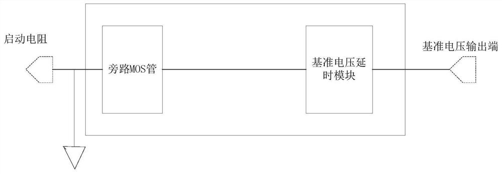
[0061] figure 1 A schematic diagram of a switching power supply protection circuit provided by an embodiment of the present invention, refer to figure 1 , the switching power supply protection circuit includes:
[0062] Reference voltage delay module and bypass MOS tube;
[0063] The input terminal of the reference voltage delay module is connected with the reference voltage output terminal (VREF) of the switching power supply control chip for time delay;
[0064] The control terminal of the bypass MOS transistor is connected to the output terminal of the reference voltage delay module, and the control voltage is provided through the charge and discharge module;
[0065] The bypass MOS transistors are also respectively connected to the startup resistor and the ground, and the bypass MOS transistors are closed to connect the startup resistors to the ground.
[0066] Specifically, in the embodiment of this application, the function of the delay of the reference voltage delay ...
Embodiment 2
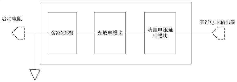
[0069] figure 2 A schematic diagram of a switching power supply protection circuit provided by an embodiment of the present invention, refer to figure 2 , the switching power supply protection circuit includes:
[0070] Reference voltage delay module, charge and discharge module and bypass MOS tube;
[0071] The input terminal of the reference voltage delay module is connected with the reference voltage output terminal (VREF) of the switching power supply control chip for time delay;
[0072] The input terminal of the charging and discharging module is connected to the output terminal of the reference voltage delay module, and the charging is performed through the reference voltage delay module;
[0073] The control terminal of the bypass MOS tube is connected to the output terminal of the charging and discharging module, and the control voltage is provided through the charging and discharging module;
[0074] The bypass MOS transistors are also respectively connected to ...
Embodiment 3
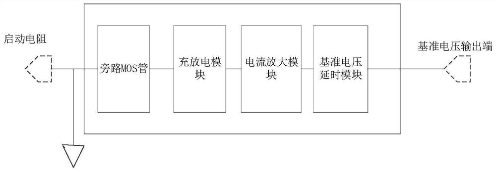
[0078] image 3 A schematic diagram of a switching power supply protection circuit provided by an embodiment of the present invention, refer to image 3 , the switching power supply protection circuit includes:
[0079] Reference voltage delay module, charge and discharge module, current amplification module and bypass MOS tube;
[0080] The input terminal of the reference voltage delay module is connected with the reference voltage output terminal (VREF) of the switching power supply control chip for time delay;
[0081] The input terminal of the current amplification module is connected to the reference voltage delay module, and the output terminal is connected to the input terminal of the charging and discharging module, which is used to increase the current output by the reference voltage delay module, that is, to increase the charging and discharging module. The charging current of the discharging module, thereby accelerating the charging speed of the charging and disch...
PUM
 Abstract
Description
Claims
Application Information