Display panel and display device
A display panel and display area technology, which is applied in the direction of identification devices, instruments, electrical components, etc., can solve the problem of poor imaging quality of the camera under the screen, and achieve the effect of enhanced imaging effect and increased light transmission area
- Summary
- Abstract
- Description
- Claims
- Application Information
AI Technical Summary
Problems solved by technology
Method used
Image
Examples
Embodiment 1
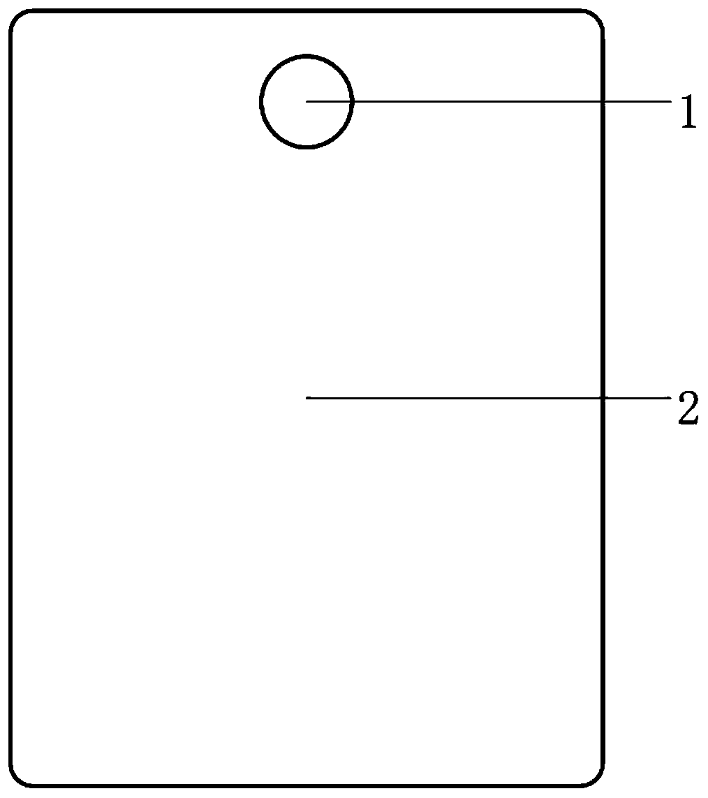
[0029] see figure 1 , this embodiment provides a display panel, figure 1 Shown is a schematic top view of the display panel provided in this embodiment. The surface of the display panel defines a functional area 1 and a display area 2. The diameter of the functional area 1 ranges from 1 to 5 mm. A camera module is arranged below the functional area. .
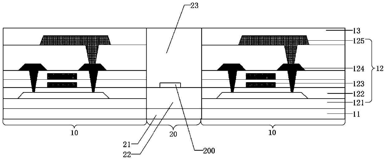
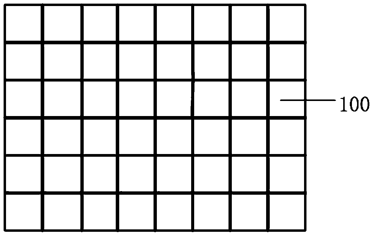
[0030] see figure 2 , image 3 and Figure 4 , the functional area 1 is provided with an array of pixels 100 , including the pixel area 10 and the light-transmitting area 20 . The pixel region 10 includes a substrate layer 11, a thin film transistor layer 12 and an encapsulation layer 13 arranged in sequence; the thin film transistor layer 12 includes a buffer layer 121, a gate insulating layer 122, a gate layer 123, and a source-drain layer 124 arranged in sequence. and the pixel electrode layer 125.
[0031] The light-transmitting region 20 includes a base substrate layer 21, an organic layer 22, a metal layer 200 and ...
Embodiment 2
[0038] This embodiment provides a display device, which includes a main body, on which the display panel according to the present invention is arranged, wherein a driving part is arranged on the main body, and the driving part can control the up and down movement of the camera to drive the light-transmitting Zone 20 transitions between a contracted state and a stretched state.
[0039] When the under-screen camera does not need to take pictures, the driver controls the camera to move downward, the light-transmitting area 20 shrinks, and the pixels 100 approach each other. The area of the pixel area 10 in the functional area 1 becomes larger, and the area of the light-transmitting area 20 becomes smaller. The pixel density in area 1 becomes larger, and the combination of functional area 1 and display area 2 realizes the complete display on the surface of the display panel. Due to the increase in PPI, the display quality of the functional area of the display panel is improv...
PUM
 Abstract
Description
Claims
Application Information
 - R&D
- Intellectual Property
- Life Sciences
- Materials
- Tech Scout
- Unparalleled Data Quality
- Higher Quality Content
- 60% Fewer Hallucinations
Browse by: Latest US Patents, China's latest patents, Technical Efficacy Thesaurus, Application Domain, Technology Topic, Popular Technical Reports.
© 2025 PatSnap. All rights reserved.Legal|Privacy policy|Modern Slavery Act Transparency Statement|Sitemap|About US| Contact US: help@patsnap.com


