Array substrate, display panel and transfer method of micro LED

An array substrate and miniature technology, which is applied to electrical components, electric solid-state devices, circuits, etc., can solve the problems of complex display panel preparation process, and achieve the effect of simplifying the setting process and simplifying the preparation process.

Active Publication Date: 2019-07-23
BOE TECH GRP CO LTD
View PDF4 Cites 20 Cited by
  • Summary
  • Abstract
  • Description
  • Claims
  • Application Information

AI Technical Summary

Problems solved by technology

[0003] This application provides a method for transferring array substrates, display panels and micro-LEDs, which can solve the problem that the preparation process of display panels is relatively complicated

Method used


Image

  • Array substrate, display panel and transfer method of micro LED
  • Array substrate, display panel and transfer method of micro LED
  • Array substrate, display panel and transfer method of micro LED

Examples


Embodiment Construction

[0070] In order to make the purpose, technical solution and advantages of the present application clearer, the implementation manners of the present application will be further described in detail below in conjunction with the accompanying drawings.

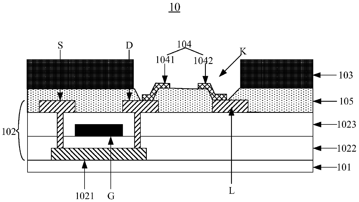
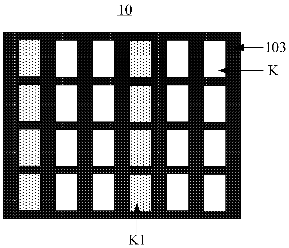
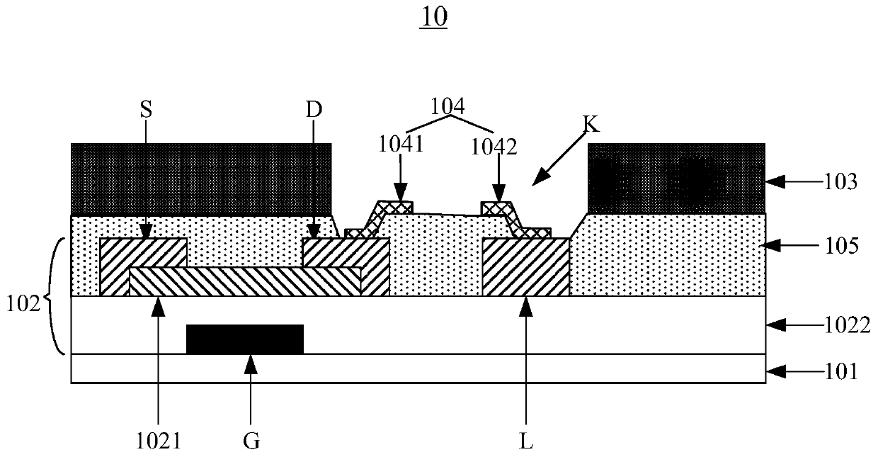
[0071] To prepare the Micro LED display panel, the Micro LED needs to be transferred to the array substrate. In the related art, an elastic die with adjustable adsorption force is used to transfer Micro LEDs. The transfer process includes: adjusting the adsorption force of the elastic die, so that the elastic die can absorb multiple Micro LEDs at one time. The multiple Micro LEDs are placed on the elastic die. The arrangement method on the array substrate is the same as the arrangement method of multiple pixel areas in the array substrate; the elastic stamper with the Micro LEDs adsorbed is moved to the top of the array substrate, and the Micro LEDs are aligned with the pixel areas on the array substrate; The adsorption force of ...


PUM


Abstract

The invention discloses an array substrate, a display panel and a transfer method of a micro LED, and belongs to the technical field of display. The array substrate comprises a substrate body, a thinfilm transistor and a pixel defining pattern, the thin film transistor and the pixel defining pattern are arranged on the substrate body in a stacked mode in the direction away from the substrate body, wherein the pixel defining pattern is provided with a through hole, a conductive structure is arranged in the through hole, the conductive structure is electrically connected with the thin film transistor, the through hole is used for accommodating the micro LED, and the thickness of the pixel defining pattern is greater than or equal to the sum of the thickness of the conductive structure and the thickness of the micro LED. The problem that the preparation process of the display panel is complex is solved. The method is used for preparing the display panel.

Description

technical field [0001] The present application relates to the field of display technology, in particular to a method for transferring an array substrate, a display panel and micro LEDs. Background technique [0002] A Micro Light-Emitting Diode (Micro LED) is a light-emitting diode whose size is in the order of microns. Due to the small size of the Micro LED, multiple Micro LED arrays can be arranged on the array substrate, so that each Micro LED can be used as a pixel on the display panel to prepare the display panel. A display panel prepared by using Micro LED may be called a Micro LED display panel. Compared with Organic Light-Emitting Diode (OLED) display panels, the service life and viewing angle of Micro LED display panels are superior to OLED display panels, so Micro LED display technology has become the focus of current research in the field of display technology. Contents of the invention [0003] The present application provides a method for transferring an arr...

Claims


Application Information

Patent Timeline
Patent Type & Authority Applications(China)
IPC IPC(8): H01L27/15H01L33/48H01L33/62H01L21/67
CPCH01L21/67144H01L27/156H01L33/486H01L33/62H01L2933/0033H01L2933/0066
Inventor 吕志军赵德江
Owner BOE TECH GRP CO LTD
Why Eureka
Try Eureka