
Multi-JTAG interface switching chip and method and single board debugging system

A technology of interface switching and chips, which is applied in the field of communication, can solve the problems of JTAG interface levels are not completely the same, unfavorable integrated board design, waste of board space, etc., to achieve low power consumption, save space, and reduce quantity Effect

Inactive Publication Date: 2019-08-02
HANGZHOU DPTECH TECH
View PDF3 Cites 8 Cited by
  • Summary
  • Abstract
  • Description
  • Claims
  • Application Information

AI Technical Summary

Problems solved by technology

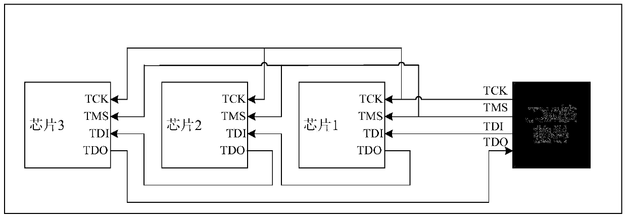
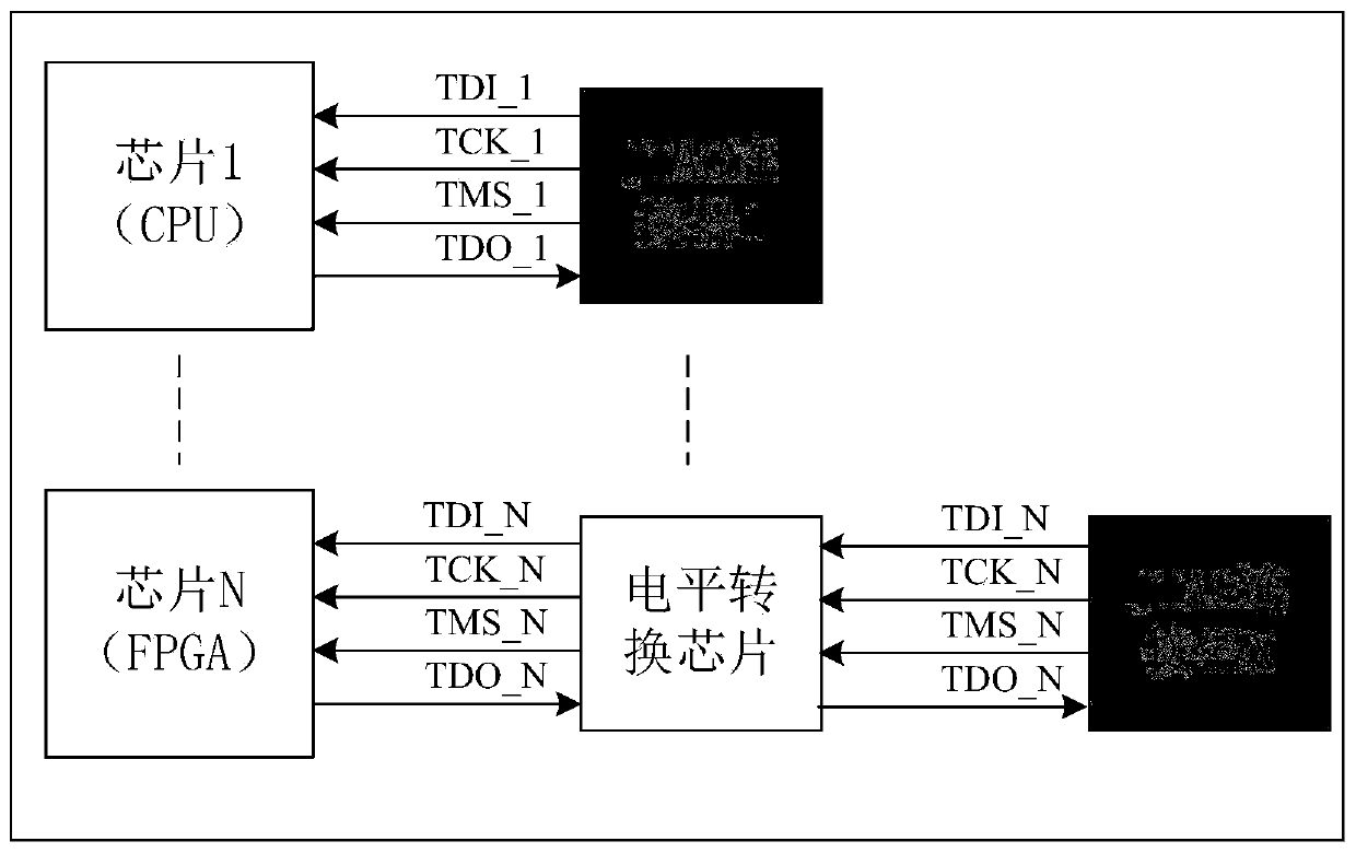
However, considering that these devices may come from different manufacturers, and the JTAG interface levels are not exactly the same, if the JTAG interface is designed in a daisy-chain series, it is necessary to add a level conversion chip. In addition, due to the JTAG debugging of each manufacturer Tools and debugging software may also be different and there may be compatibility issues
If each device uses a JTAG connector, it will waste the board space of the board, which is not conducive to the design of the board with high integration

Method used


Image

  • Multi-JTAG interface switching chip and method and single board debugging system
  • Multi-JTAG interface switching chip and method and single board debugging system
  • Multi-JTAG interface switching chip and method and single board debugging system

Examples


Embodiment Construction

[0025] Reference will now be made in detail to the exemplary embodiments, examples of which are illustrated in the accompanying drawings. When the following description refers to the accompanying drawings, the same numerals in different drawings refer to the same or similar elements unless otherwise indicated. The implementations described in the following exemplary examples do not represent all implementations consistent with this specification. Rather, they are merely examples of apparatuses and methods consistent with aspects of the present specification as recited in the appended claims.

[0026] The terms used in this specification are for the purpose of describing particular embodiments only, and are not intended to limit the specification. As used in this specification and the appended claims, the singular forms "a", "the", and "the" are intended to include the plural forms as well, unless the context clearly dictates otherwise. It should also be understood that the t...


PUM


Abstract

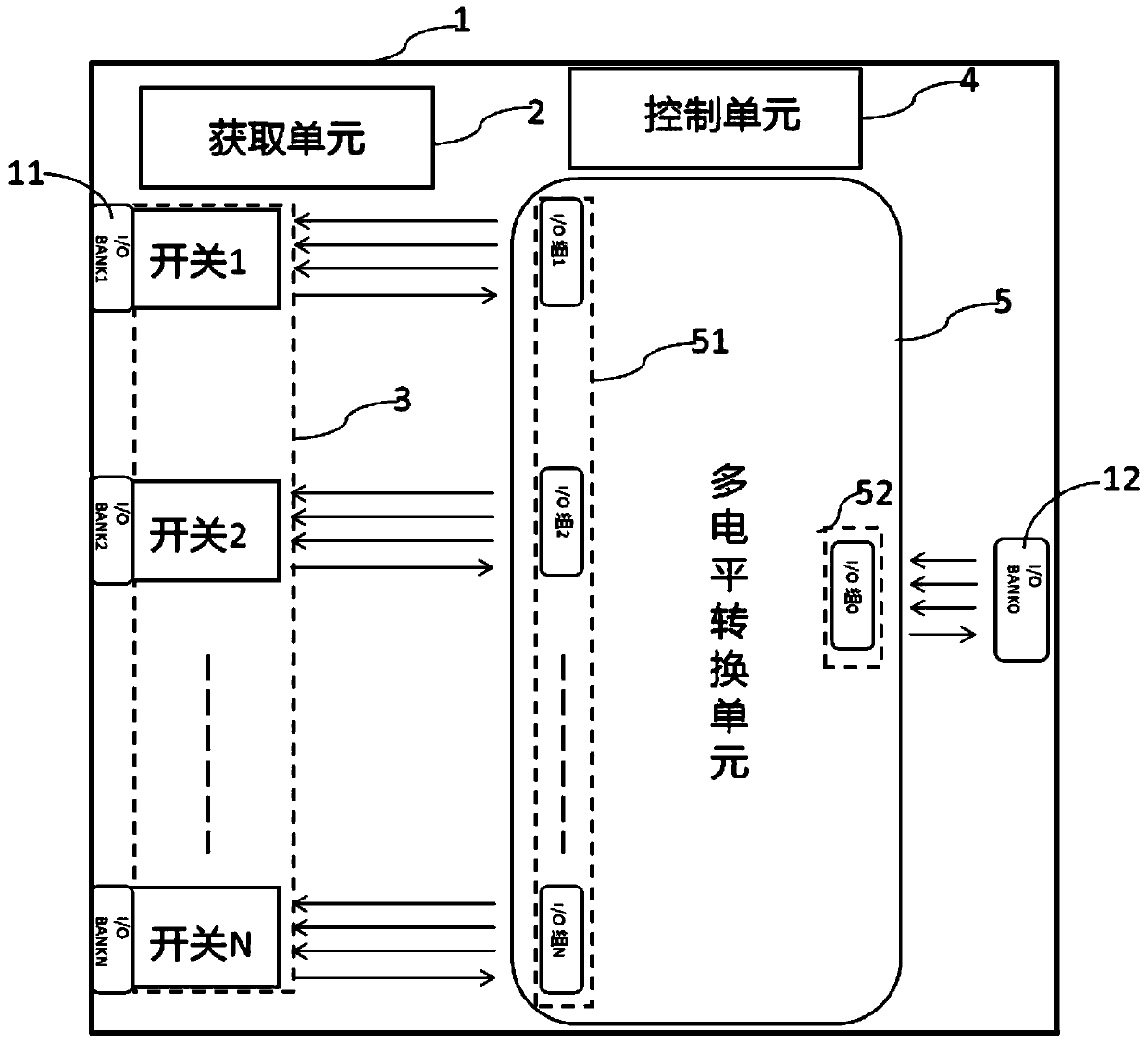
The invention provides a multi-JTAG (joint test action group) interface switching chip, a multi-JTAG interface switching method and a single-board debugging system. The chip can be a CPLD (complex programmable logic device) and comprises a plurality of first input / output interface groups, a plurality of second input / output interface groups and a processing unit, wherein each first input / output interface group is connected with a JTAG interface of a chip to be tested, and the second input / output interface group is connected with a JTAG connector; and the processing unit is used for acquiring acurrent channel gating signal and controlling a channel between the first input / output interface group and the second input / output interface group corresponding to the channel gating signal to be conducted according to the channel gating signal. The chip is used for switching the JTAG interfaces of different chips to be tested to the JTAG connectors connected with the JTAG cables, so that the number of the JTAG connectors on a single board is reduced, the space of the single board is saved, and the cost is reduced. And the control mode is simple, and the CPLD circuit is low in power consumption and high in stability.

Description

technical field [0001] This specification relates to the field of communication technology, in particular to a multi-JTAG interface switching chip, method and single-board debugging system. Background technique [0002] CPLD (Complex Programmable Logic Device) complex programmable logic device is a relatively large-scale integrated digital circuit with complex structure. CPLD is a digital integrated circuit in which users can construct logic functions according to their own needs. The basic design method is to use the integrated development software platform to generate the corresponding object code file by means of schematic diagram and hardware description language, and then download the object code to the chip through the download cable to realize the design of the digital system. [0003] JTAG (Joint Test Action Group; Joint Test Working Group) is an international standard test protocol (IEEE 1149.1 compatible), mainly used for chip internal testing. Most of the advanc...

Claims


Application Information

Patent Timeline
IPC IPC(8): G06F13/38
CPCG06F13/385Y02D10/00
Inventor 冯永刚
Owner HANGZHOU DPTECH TECH
Learn More