Optical fingerprint identification circuit and array

A fingerprint recognition, circuit array technology, applied in character and pattern recognition, acquisition/organization of fingerprints/palmprints, instruments, etc., can solve problems such as low brightness and weak photoelectric current of optical sensors

Inactive Publication Date: 2019-08-06
WUHAN CHINA STAR OPTOELECTRONICS TECH CO LTD
View PDF9 Cites 14 Cited by
  • Summary
  • Abstract
  • Description
  • Claims
  • Application Information

AI Technical Summary

Problems solved by technology

However, due to the low brightness of the OLED screen, the light from the OLED screen is used to trigger the optical sensor, result

Method used


Image

  • Optical fingerprint identification circuit and array
  • Optical fingerprint identification circuit and array
  • Optical fingerprint identification circuit and array

Examples


Embodiment Construction

[0025] The technical solutions in the embodiments of the present invention will be clearly and completely described below in conjunction with the drawings in the embodiments of the present invention. Obviously, the described embodiments are only a part of the embodiments of the present invention, rather than all the embodiments. Based on the embodiments of the present invention, all other embodiments obtained by those skilled in the art without creative work shall fall within the protection scope of this application.

[0026] The description of the following embodiments refers to the attached drawings to illustrate specific embodiments that the present invention can be implemented.

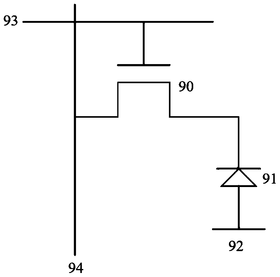
[0027] Such as figure 1 As shown, it is a schematic diagram of an existing optical fingerprint identification circuit. The optical fingerprint identification circuit includes a transistor 90, a photodiode 91, a diode bias 92, a scanning line 93, and a reading line 94.

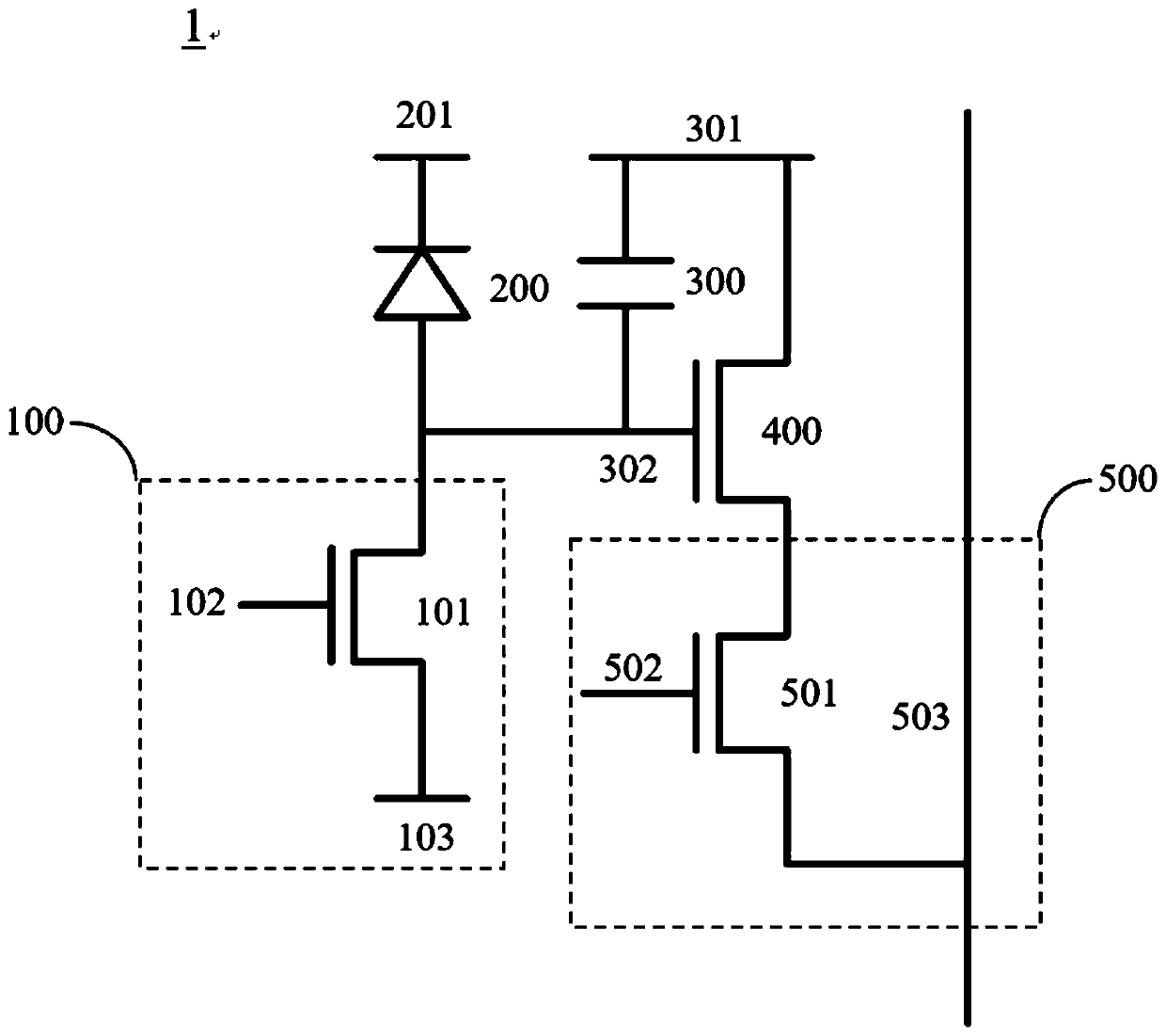
[0028] Such as figure 2 As shown...


PUM


Abstract

An optical fingerprint identification circuit comprises a reset unit, a photodiode, a storage capacitor, an amplification transistor and a data writing unit. The reset unit comprises a reset transistor, a reset signal line and a reset voltage end and is used for resetting the grid electrode of the amplification transistor; the photodiode is used for receiving an optical signal to generate a photocurrent and outputting the photocurrent to the storage capacitor; the amplifying transistor is used for amplifying a signal received by the amplifying transistor and outputting the signal to the data writing unit.

Description

[0001] 【Technical Field】 [0002] The invention relates to the field of display technology, in particular to an optical fingerprint identification circuit and an array. [0003] 【Background technique】 [0004] Optical fingerprint recognition technology has become a mature fingerprint recognition technology and has been widely used in people's daily life, such as fingerprint locks and fingerprint attendance machines. [0005] At present, due to the emergence of in-screen fingerprint recognition applications in smart phones, based on organic light emitting diode (OLED) screens, optical fingerprint recognition systems can omit complex and bulky optical systems. However, due to the low brightness of the OLED screen, the light of the OLED screen triggers the optical sensor, which causes the photo-generated current of the optical sensor to be relatively weak, which is a challenge for signal collection and processing. [0006] [Content of the invention] [0007] The purpose of the present inven...

Claims


Application Information

Patent Timeline
IPC IPC(8): G06K9/00
CPCG06V40/1318
Inventor 肖军城田超
Owner WUHAN CHINA STAR OPTOELECTRONICS TECH CO LTD
Why Eureka
Try Eureka