A kind of multi-layer composite protective layer applied to PCB and method

A multi-layer composite and protective layer technology, applied in the direction of coating non-metallic protective layers, printed circuits, electrical components, etc., can solve the problems of easily damaged electronic components, long colloid curing time, and high cost of potting glue, and achieves a high technological Simple, improve the degree of automated production of products, and save labor costs

Active Publication Date: 2020-09-25
康威通信技术股份有限公司
View PDF8 Cites 0 Cited by
  • Summary
  • Abstract
  • Description
  • Claims
  • Application Information

AI Technical Summary

Problems solved by technology

[0003] At present, the PCB sealing and protection methods that work in underwater, humid, and hot environments mainly use conformal paint and potting glue to completely cover and seal the PCB. The thickness is relatively high, resulting in excessive weight of the product.
The inventors found that this method occupies the limited structural space of other parts, and the curing time of the colloid is long, the PCB size consumes a high cost of potting glue, and the follow-up maintenance needs to buckle the glue and dissolve the colloid. It is easy to damage electronic components, which is not conducive to the recovery and analysis of fault phenomena

Method used


Image

  • A kind of multi-layer composite protective layer applied to PCB and method
  • A kind of multi-layer composite protective layer applied to PCB and method
  • A kind of multi-layer composite protective layer applied to PCB and method

Examples


Embodiment 1

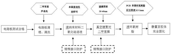
[0039] (1) First, use xylene to clean the PCB and components, and clean the rosin, flux, oil and other sundries on the surface of the PCB.

[0040](2) The PCB is baked in an oven using a dehumidification process, and the moisture absorbed by the PCB and components during the storage and circulation process is discharged.

[0041] (3) Immerse the PCB in the nanomaterial silica solution. After the surface of the PCB is completely debubbled, take out the PCB and dry it.

[0042] (4) A vacuum coating machine is used to vacuum coat the PCB by chemical vapor deposition. Among them, the coating machine and coating materials are all used in Shanghai Paraleng Coating Machine, using Paryleng C material. Coating thickness is 30um.

[0043] (5) Immerse the PCB in epoxy resin, repeatedly immerse in YF-3508 epoxy resin, the thickness is about 0.5mm, and wait for the colloid to solidify.

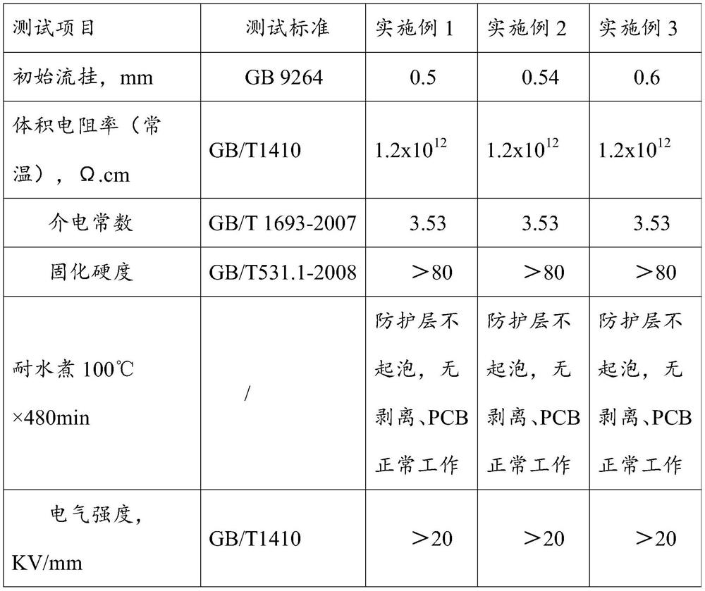
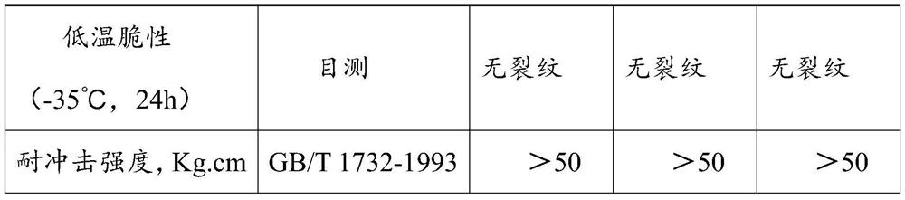
[0044] The above-mentioned composite protective layer was tested, and the results are shown in Table...

Embodiment 2

[0049] (1) First, use xylene to clean the PCB and components, and clean the rosin, flux, oil and other sundries on the surface of the PCB.

[0050] (2) The PCB is baked in an oven using a dehumidification process, and the moisture absorbed by the PCB and components during the storage and circulation process is discharged.

[0051] (3) Immerse the PCB in a nanomaterial silica solution with a particle size of 7-30nm. After the surface of the PCB is completely debubbled, take out the PCB and let it dry for 3-5 minutes to obtain a film layer of 500-1000nm.

[0052] (4) A vacuum coating machine is used to vacuum coat the PCB by chemical vapor deposition. Among them, the coating machine and coating materials are all used in Shanghai Paraleng Coating Machine, using Paryleng C material. Coating thickness is 35um.

[0053] (5) Immerse the PCB in epoxy resin, repeatedly immerse in YF-3508 epoxy resin, the thickness is about 0.7mm, and wait for the colloid to solidify.

Embodiment 3

[0055] (1) First, use xylene to clean the PCB and components, and clean the rosin, flux, oil and other sundries on the surface of the PCB.

[0056] (2) The PCB is baked in an oven using a dehumidification process, and the moisture absorbed by the PCB and components during the storage and circulation process is discharged.

[0057] (3) Immerse the PCB in a nanomaterial silica solution with a particle size of 7-30. After the surface of the PCB is completely debubbled, take out the PCB and let it dry for 3-5 minutes to obtain a film layer of 500-1000nm.

[0058] (4) A vacuum coating machine is used to vacuum coat the PCB by chemical vapor deposition. Among them, the coating machine and the coating material are all used in the coating machine of Shanghai Paraleng, and the material of Paryleng C is used, and the coating thickness is 40um.

[0059] (5) Immerse the PCB in epoxy resin, repeatedly immerse in YF-3508 epoxy resin, the thickness is about 1mm, and wait for the colloid to ...


PUM

PropertyMeasurementUnit
thicknessaaaaaaaaaa
thicknessaaaaaaaaaa
particle diameteraaaaaaaaaa

Abstract

The invention relates to a multi-layer composite protection layer applied to PCB and a method. The multi-layer composite protection layer comprises a nano silicon dioxide coating, Parylene C coating,and epoxy resin coating which are arranged inside to outside, and the thickness of the Parylene C coating is 30-40 [mu]m. The application method comprises the steps of: 1) cleaning and dehumidifying the surface of a PCB; 2) socking the cleaned PCB into a nanosilicon dioxide liquid to obtain a PCB with a surface coated with nanosilicon dioxide; 3) coating a Parylene C material at the surface of thePCB with the surface coated with nanosilicon dioxide by employing a vacuum chemical vapor deposition method; and 4) obtaining the epoxy resin material at the surface of the PCB obtained in the step 3). The PCB is good in waterproof performance, can normally work in a soaking environment and has a good mechanical performance.

Description

technical field [0001] The invention belongs to the technical field of preparation of waterproof sealing materials, and in particular relates to a multilayer composite protective layer applied to PCBs and a method thereof. Background technique [0002] The information disclosed in this background section is only intended to increase the understanding of the general background of the present invention, and is not necessarily taken as an acknowledgment or any form of suggestion that the information constitutes the prior art already known to those skilled in the art. [0003] At present, the PCB sealing and protection methods that work in underwater, humid, and hot environments mainly use conformal paint and potting glue to completely cover and seal the PCB with a relatively high thickness, resulting in excessive weight of the product. The inventors found that this method occupies the limited structural space of other parts, and the curing time of the colloid is long, the PCB s...

Claims


Application Information

Patent Timeline
Patent Type & Authority Patents(China)
IPC IPC(8): H05K3/28
CPCH05K3/284H05K3/285H05K2203/1322H05K2203/1377
Inventor 王军冯建业张明广杨震威
Owner 康威通信技术股份有限公司
Why Eureka
Try Eureka