Non-contact card chip testing device, testing method and non-contact card chip

A non-contact card and chip testing technology, which is applied in electronic circuit testing, radio frequency circuit testing, recording carriers used by machines, etc., can solve problems such as poor anti-interference ability and long testing time

Pending Publication Date: 2019-08-16
SHANDONG HUAYI MICRO ELECTRONICS
View PDF6 Cites 0 Cited by
  • Summary
  • Abstract
  • Description
  • Claims
  • Application Information

AI Technical Summary

Problems solved by technology

[0005] This application provides a non-contact card chip testing device, testing method and non-contact card chip to solve the problems of long testing time and poor anti-interference ability in the testing process in the prior art

Method used


Image

  • Non-contact card chip testing device, testing method and non-contact card chip
  • Non-contact card chip testing device, testing method and non-contact card chip
  • Non-contact card chip testing device, testing method and non-contact card chip

Examples


Embodiment 1

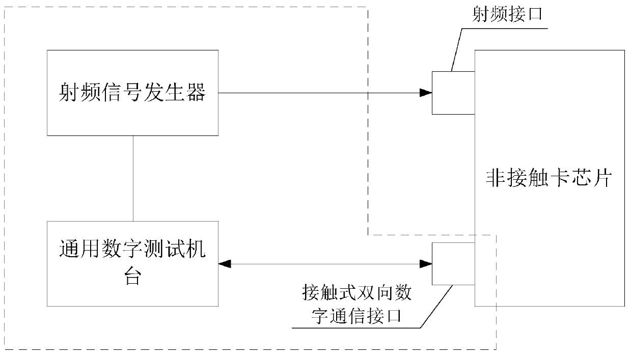
[0041] see figure 2 , figure 2 It is a schematic structural diagram of the non-contact card chip testing device provided by the embodiment of the present application. Depend on figure 2 It can be seen that the non-contact card chip testing device mainly includes three parts: a general digital testing machine, a radio frequency signal generator and a contact bidirectional digital communication interface. Wherein, the contact-type two-way digital communication interface is set on the non-contact card chip. The universal digital test machine is used to control the radio frequency signal generator to send a certain frequency carrier, and the universal digital test machine controls the opening and closing of the radio frequency signal generator. The general digital testing machine is connected with the contact-type two-way digital communication interface of the non-contact card chip, and is used for transmitting baseband signals. The radio frequency signal generator communic...

Embodiment 2

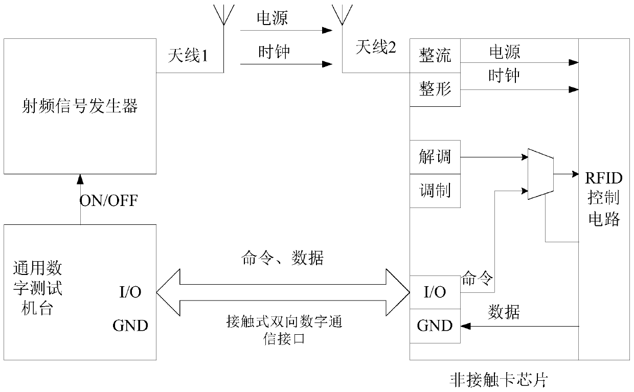
[0052] exist figure 2 with image 3 On the basis of the illustrated embodiment see Figure 4 , Figure 4 It is a schematic flow chart of the contactless card chip testing method provided in the embodiment of the present application. The test method in this embodiment is applied to a non-contact card chip testing device, which mainly includes: a general-purpose digital test machine and a radio frequency signal generator, and the non-contact card chip to be tested is provided with a radio frequency interface.

[0053] Depend on Figure 4 As can be seen, the test method in this embodiment includes the following steps:

[0054] S1: Set a contact-type bidirectional digital communication interface on the contactless card chip to set the transmission mode of the test signal.

[0055] Among them, the test signal includes: baseband signal, power signal and clock signal, the baseband signal includes: command, first data and second data, the first data is the test data sent by the ...


PUM


Abstract

The invention discloses a non-contact card chip testing device, a non-contact card chip testing method and a non-contact card chip. The testing device comprises a universal digital testing machine table, a radio frequency signal generator and a contact type bidirectional digital communication interface, the universal digital testing machine table is in communication connection with the contact type bidirectional digital communication interface, and the radio frequency signal generator is in communication connection with the radio frequency interface. The method comprises the following steps: setting a transmission mode of a test signal by arranging a contact-type bidirectional digital communication interface on a non-contact card chip, and sending a power supply and a clock signal to the non-contact card chip through a radio frequency interface; transmitting a baseband signal to the non-contact card chip through the contact type bidirectional digital communication interface; and enabling the contactless card chip to return the second data by decoding and encoding. The non-contact card chip comprises a contact type bidirectional digital communication interface which is used for transmitting baseband signals. According to the invention, the chip test efficiency can be improved, the test anti-interference capability can be improved, and the test cost can be reduced.

Description

technical field [0001] The application relates to the technical field of chip testing, in particular to a non-contact card chip testing device, a testing method and a non-contact card chip. Background technique [0002] The contactless card chip is a kind of chip that obtains power through the antenna and electromagnetic field, and communicates with the card reader. For contactless card manufacturers, in order to ensure the factory quality of the contactless card chip, it is necessary to test whether the function of the contactless card chip is normal before leaving the factory, which requires the testing equipment of the contactless card chip. [0003] The current contactless card test equipment is usually a dedicated radio frequency test machine, which uses modulated radio frequency to send commands to the chip to be tested and receive the returned information from the chip to be tested. The baseband signal, clock, and energy of the chip to be tested All are obtained thro...

Claims


Application Information

Patent Timeline
Patent Type & Authority Applications(China)
IPC IPC(8): H04B17/00G01R31/28G06K19/077
CPCH04B17/00H04B17/0085G01R31/2822G06K19/07749
Inventor 王光春曾为民李向宏
Owner SHANDONG HUAYI MICRO ELECTRONICS
Why Eureka
Try Eureka