Printed circuit board, manufacturing method thereof and electronic equipment

A printed circuit board and circuit board technology, applied in the electronic field, can solve the problems of small resistance to stress and deformation, affect welding reliability, and reduce support, so as to achieve firm solder joints, improve welding reliability, and improve service life.

Inactive Publication Date: 2019-08-20
HUAWEI TECH CO LTD
View PDF8 Cites 12 Cited by
  • Summary
  • Abstract
  • Description
  • Claims
  • Application Information

AI Technical Summary

Problems solved by technology

Since the frame printed circuit board 030 is a hollow structure, its ability to resist stress and deformation is relatively small, and it is easy to form a larger warp when subjected to stress
When the warpage of the frame PCB 030 is high, it will reduce the supporting effect of the frame PCB 030 on the top PCB 010 and the bottom PCB 020, which may affect the frame PCB 030 and the top PCB 010. and the soldering reliability of the underlying printed circuit board 020, resulting in open soldering of solder joints and failure of electrical connections

Method used


Image

  • Printed circuit board, manufacturing method thereof and electronic equipment
  • Printed circuit board, manufacturing method thereof and electronic equipment
  • Printed circuit board, manufacturing method thereof and electronic equipment

Examples


Embodiment Construction

[0047] The technical solutions in the embodiments of the present invention will be clearly described below in conjunction with the accompanying drawings. Apparently, the described embodiments are only some of the embodiments of the present invention, but not all of them. Based on the embodiments of the present invention, all other embodiments obtained by persons of ordinary skill in the art without making creative efforts belong to the protection scope of the present invention.

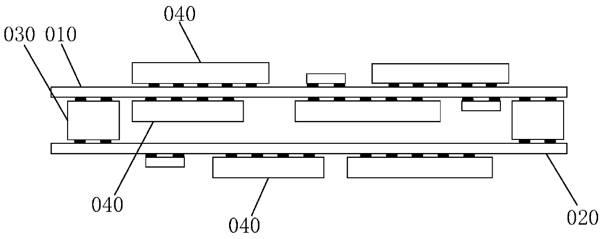
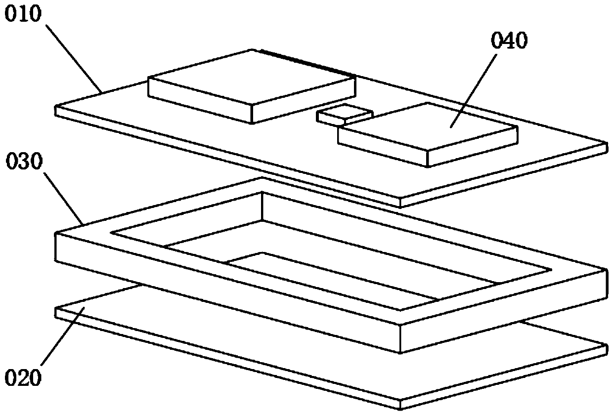
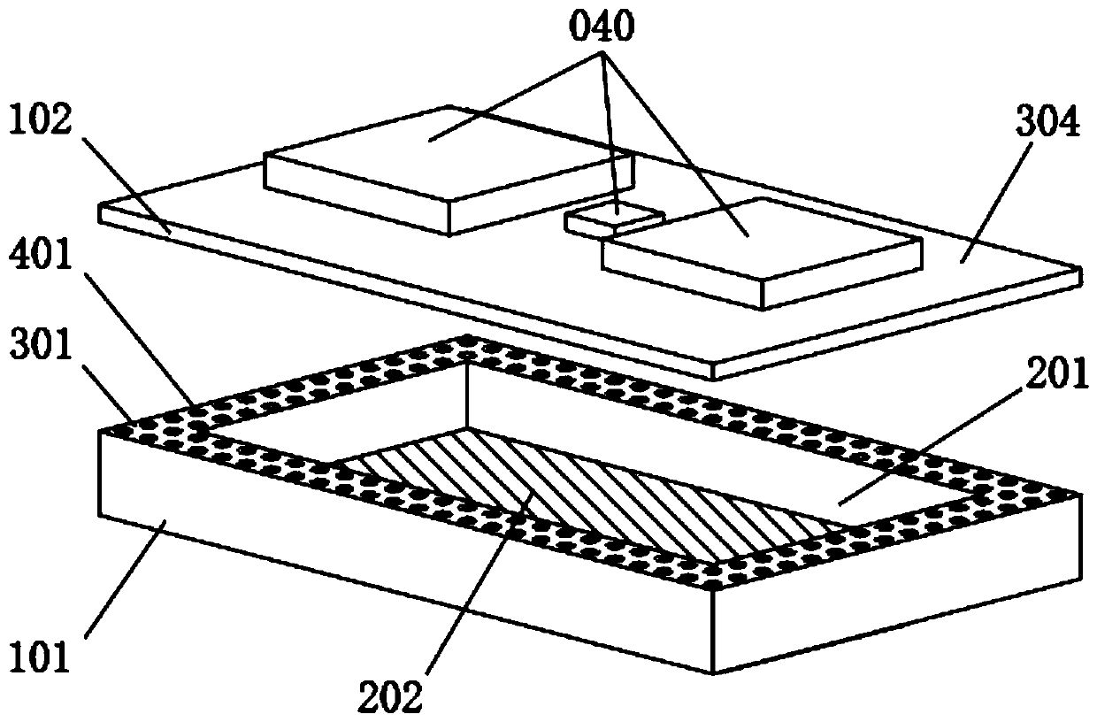
[0048] Figure 2a An exploded view of the structure of a printed circuit board provided by an embodiment of the present invention. Figure 2b A schematic cross-sectional view of a printed circuit board provided by an embodiment of the present invention. Such as Figure 2a and Figure 2b As shown, the printed circuit board includes a first printed circuit board 101 and a second printed circuit board 102. Wherein, the first printed circuit board 101 includes a first surface 301 and a second surface...


PUM


Abstract

The embodiment of the invention provides a printed circuit board, a manufacturing method thereof and electronic equipment. The printed circuit board comprises a first printed circuit board. The firstprinted circuit board comprises a first surface and a second surface, and the first surface and the second surface are opposite in direction. The first printed circuit board is provided with a first groove, and an opening of the first groove faces the first surface. The first surface is provided with a first bonding pad. An electronic element is mounted on the second surface. The printed circuit board also comprises a second printed circuit board which comprises a third surface and a fourth surface, and the third surface and the fourth surface are opposite in direction. The third surface is provided with a second bonding pad, and the second bonding pad corresponds to the first bonding pad in position. The third surface and the fourth surface are respectively provided with electronic elements. The first printed circuit board and the second printed circuit board are welded through the first bonding pad and the second bonding pad to form a stacked structure. The printed circuit board provided by the invention is not likely to warp, has stronger stress deformation resistance, and can prolong the service life of electronic equipment.

Description

technical field [0001] The present application relates to the field of electronic technology, in particular to a printed circuit board, a manufacturing method thereof, and electronic equipment. Background technique [0002] In miniaturized electronic equipment, due to the small size of the equipment, the available space inside the equipment is very limited. In a limited space, electronic equipment usually needs to accommodate components such as screens, batteries, printed circuit boards, camera modules, vibration motors, etc., so there are high requirements for the effective use of electronic equipment space; With the continuous improvement of performance, there needs to be enough space inside the electronic device to accommodate a battery with a larger capacity to ensure battery life. [0003] In order to save the internal space of electronic equipment, some current electronic equipment uses double-layer printed circuit boards. Figure 1a is a schematic cross-sectional vie...

Claims


Application Information

Patent Timeline
Patent Type & Authority Applications(China)
IPC IPC(8): H05K1/14H05K3/36
CPCH05K1/144H05K3/368
Inventor 乔建文任红强邓凌超
Owner HUAWEI TECH CO LTD
Why Eureka
Try Eureka