An organic light emitting display device
A technology of light-emitting display and organic light-emitting layer, applied in diodes, semiconductor devices, electrical components, etc., can solve the problem of light loss as high as one-half, achieve high color gamut, suppress bad halo, and improve brightness.
- Summary
- Abstract
- Description
- Claims
- Application Information
AI Technical Summary
Problems solved by technology
Method used
Image
Examples
Embodiment 1
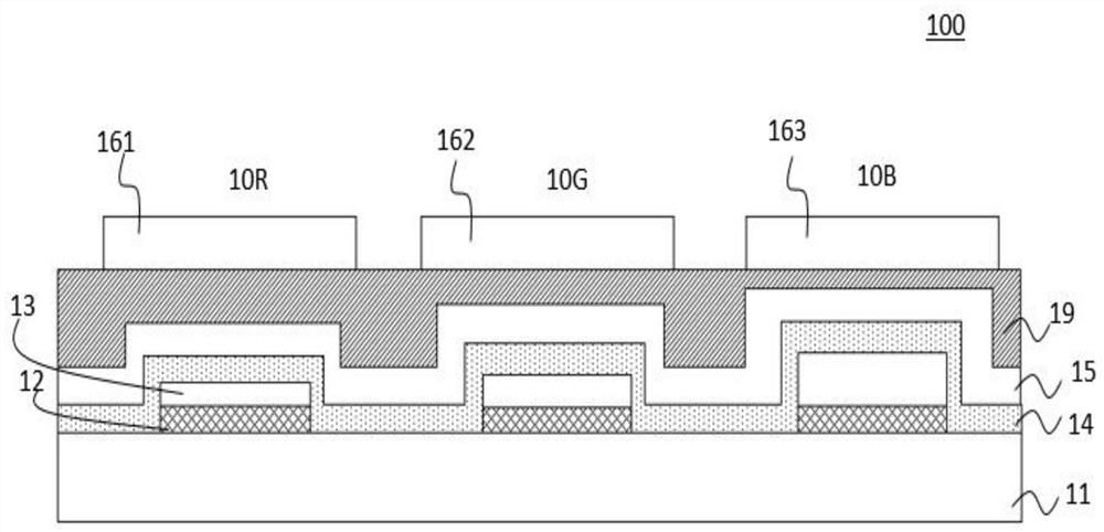
[0020] figure 1 For the schematic diagram of the organic light-emitting display device provided in Embodiment 1 of the present invention, please refer to figure 1 , the organic light-emitting display device 100 includes a plurality of OLED display units 10, and each OLED display unit 10 includes an anode 12 disposed on a substrate 11, an optical adjustment layer 13 disposed on the anode 12, an organic light-emitting diode disposed on the optical adjustment layer 13 The light emitting layer 14 and the cathode layer 15 disposed on the organic light emitting layer 14 . Wherein, the organic light-emitting layer 14 is a common layer of a plurality of OLED display units, the anode 12 is a reflective metal layer, the cathode layer 15 is a transflective metal, and the thickness of the optical adjustment layer 13 of the OLED display unit 10 that emits light of different colors different. A film layer 19 may also be provided on the upper layer of the cathode layer 15 to play the role ...
Embodiment 2
[0036] Please refer to Figure 9 , is a schematic diagram of an organic light-emitting display device provided in Embodiment 2 of the present invention. The organic light-emitting display device 200 includes a plurality of OLED display units 20, and each OLED display unit 20 includes an anode 22 arranged on a substrate 21, and an anode 22 arranged on the anode 22. The optical adjustment layer 23, the first organic light emitting unit 24 disposed on the optical adjustment layer 23, the intermediate layer 25 disposed on the first organic light emitting unit 24, the second organic light emitting unit 26 disposed on the intermediate layer 25, and the second organic light emitting unit 26 disposed on the second organic light emitting unit On the cathode layer 27 on the organic light emitting unit 26, a film layer 29 may also be provided on the cathode layer 27 for flattening or improving the effect of light extraction. Wherein, the light-emitting layer in the first organic light-em...
PUM
| Property | Measurement | Unit |
|---|---|---|
| width | aaaaa | aaaaa |
| width | aaaaa | aaaaa |
| thickness | aaaaa | aaaaa |
Abstract
Description
Claims
Application Information


