Array substrate and manufacturing method thereof

An array substrate and array layer technology, applied in nonlinear optics, instruments, optics, etc., can solve the problems of uneven display around the display panel, affecting display quality, etc., to achieve improved display quality, good display quality, and reduced leveling Effect

Inactive Publication Date: 2019-08-27
SHENZHEN CHINA STAR OPTOELECTRONICS TECH CO LTD
View PDF6 Cites 6 Cited by
  • Summary
  • Abstract
  • Description
  • Claims
  • Application Information

AI Technical Summary

Problems solved by technology

In the standard design, the height of the main spacer 871 and the edge spacer 873 are generally set to be the same, but because the material film of the spacer is generally a photoresist material with leveling properties, the material film of the spacer is in the color resistance of the edge. The part above the block 842 is thinner than the part above the color resist...

Method used


Image

  • Array substrate and manufacturing method thereof
  • Array substrate and manufacturing method thereof
  • Array substrate and manufacturing method thereof

Examples


Embodiment Construction

[0035]In order to further illustrate the technical means and effects adopted by the present invention, the following describes in detail in conjunction with preferred embodiments of the present invention and accompanying drawings.

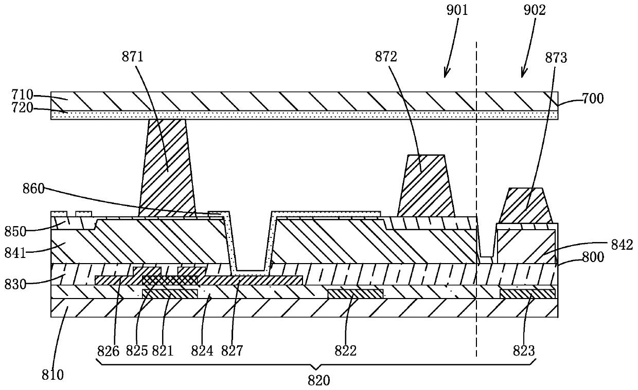
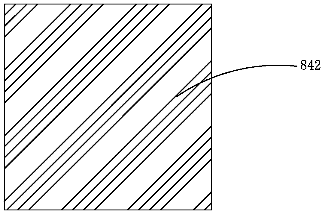
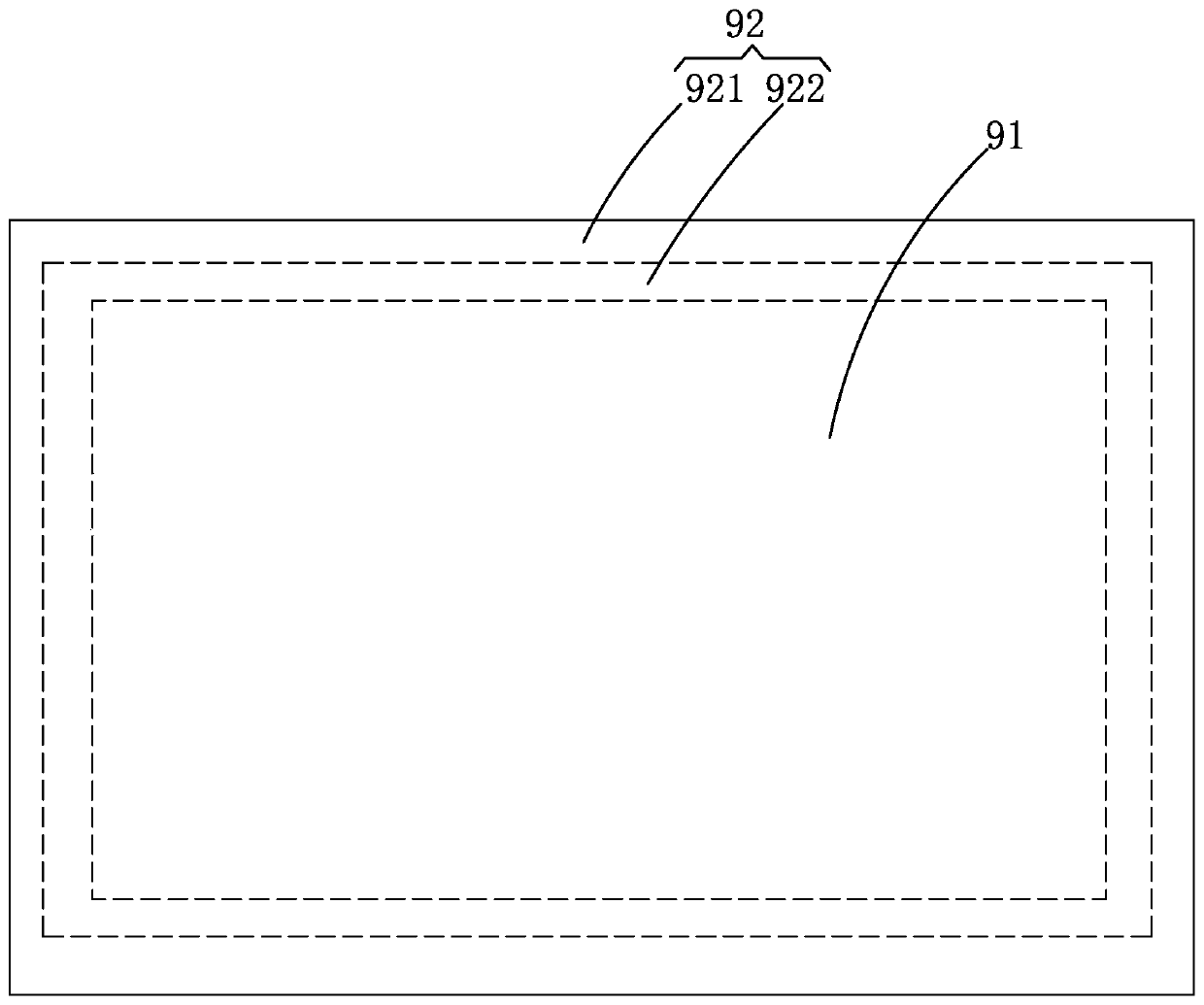
[0036] The present invention provides an array substrate using POA technology, please refer to image 3 , the array substrate has a display area 91 and a peripheral area 92 located outside the display area 91 . Please combine image 3 and Figure 4 The array substrate includes an edge color-resist pattern 32 disposed in the peripheral area 92 and an edge spacer 42 located above the edge color-resist pattern 32 . Please combine Figure 4 and Figure 5 The edge color-resist pattern 32 includes a block portion 321 and a retaining wall 322 located outside the block portion 321 .

[0037] Specifically, in Figure 4 In the illustrated embodiment, the array substrate further includes a base substrate 10, a thin film transistor array layer 20 dispose...


PUM


Abstract

The invention provides an array substrate and a manufacturing method thereof. The array substrate comprises a display area and a peripheral area located at the outer side of the display area; the array substrate comprises an edge color resistance pattern arranged in the peripheral area and an edge spacer arranged above the edge color resistance pattern; the edge color resistance pattern comprisesa block portion and a retaining wall located at the outer side of the block portion, so that when a spacer material layer used for manufacturing a main spacer and the edge spacer is formed above a display area color resistance pattern and the edge color resistance pattern of the display area, the levelling property of the part, above the edge color resistance pattern, of the spacer material layeris greatly reduced, so that the height difference between the main spacer which is finally formed above the display area color resistance pattern and the edge spacer located above the edge color resistance pattern is reduced, and the display quality of a liquid crystal display panel can be improved.

Description

technical field [0001] The present invention relates to the field of display technology, in particular to an array substrate and a manufacturing method thereof. Background technique [0002] Liquid crystal display (Liquid Crystal Display, LCD) has many advantages such as thin body, power saving, and no radiation, and has been widely used, such as: mobile phones, personal digital assistants (PDA), digital cameras, computer screens and notebook computers screen etc. [0003] Most of the liquid crystal display devices currently on the market are backlight liquid crystal display devices, which include a housing, a liquid crystal display panel disposed in the housing, and a backlight module disposed in the housing. The structure of a traditional liquid crystal display panel is composed of a color filter substrate (Color Filter), a thin film transistor array substrate (Thin FilmTransistor Array Substrate, TFT Array Substrate), and a liquid crystal layer (Liquid Crystal Layer) arr...

Claims


Application Information

Patent Timeline
IPC IPC(8): G02F1/1339G02F1/1362
CPCG02F1/13394G02F1/1362G02F1/136222
Inventor 叶成亮
Owner SHENZHEN CHINA STAR OPTOELECTRONICS TECH CO LTD
Why Eureka
Try Eureka