Supercharge Your Innovation With Domain-Expert AI Agents!

A thin film growth component, method and LED preparation method

A thin film growth and component technology, applied in electrical components, semiconductor devices, circuits, etc., can solve problems such as large lattice stress and poor performance of LED devices, and achieve the effect of improving lattice stress, improving performance, and ensuring film quality

Active Publication Date: 2021-03-16
XIAMEN CHANGELIGHT CO LTD
View PDF8 Cites 0 Cited by
  • Summary
  • Abstract
  • Description
  • Claims
  • Application Information

AI Technical Summary

Problems solved by technology

[0005] In view of this, the present invention provides a thin film growth component, method and LED preparation method to solve the problem of poor performance of LED devices due to the large lattice stress between the existing ALN buffer layer and the GaN film

Method used


Image

  • A thin film growth component, method and LED preparation method
  • A thin film growth component, method and LED preparation method
  • A thin film growth component, method and LED preparation method

Examples


Embodiment Construction

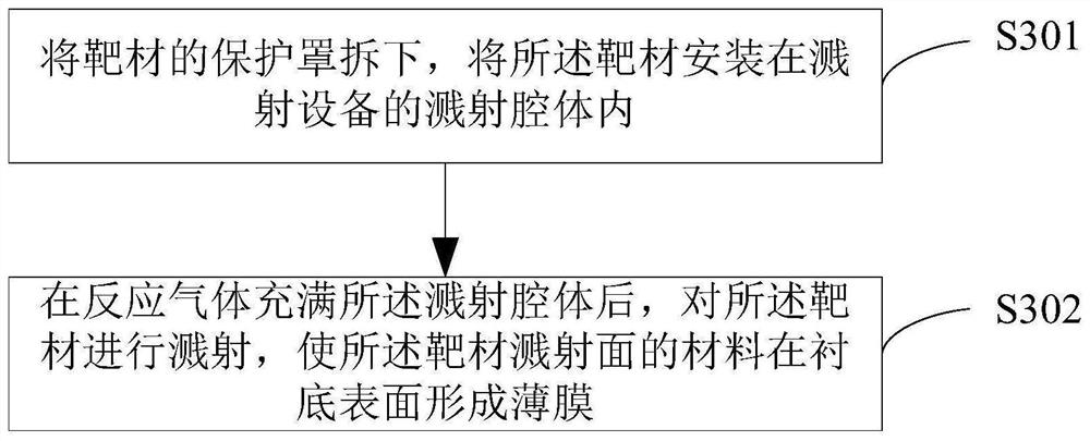
[0032] As mentioned in the background art, there is a huge lattice stress between the ALN buffer layer and the GaN thin film, which makes the performance of the LED device poor. The inventors found that the use of an AlGaN buffer layer can effectively improve the lattice stress of the GaN film. However, when an AlGaN buffer layer is fabricated by using an AlGa alloy target material, since the AlGa alloy is easily oxidized by water and oxygen in the air, the quality of the formed AlGaN buffer layer film is poor.

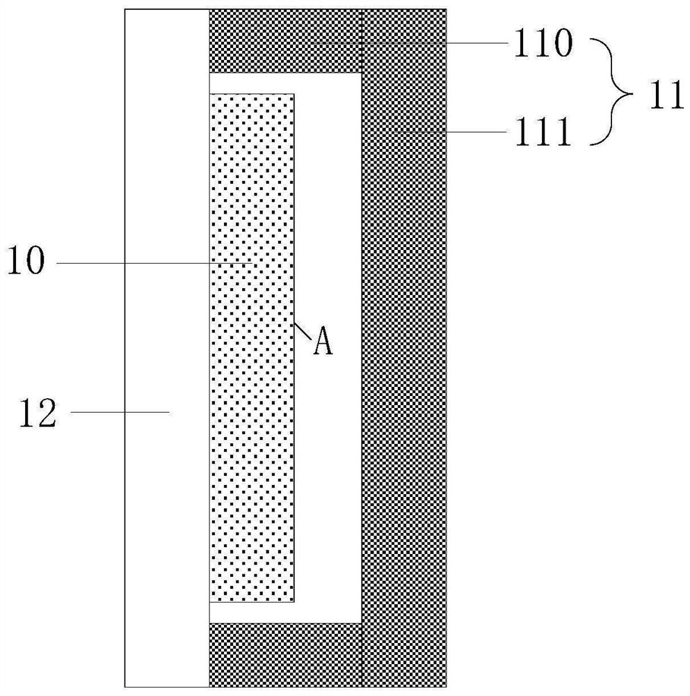
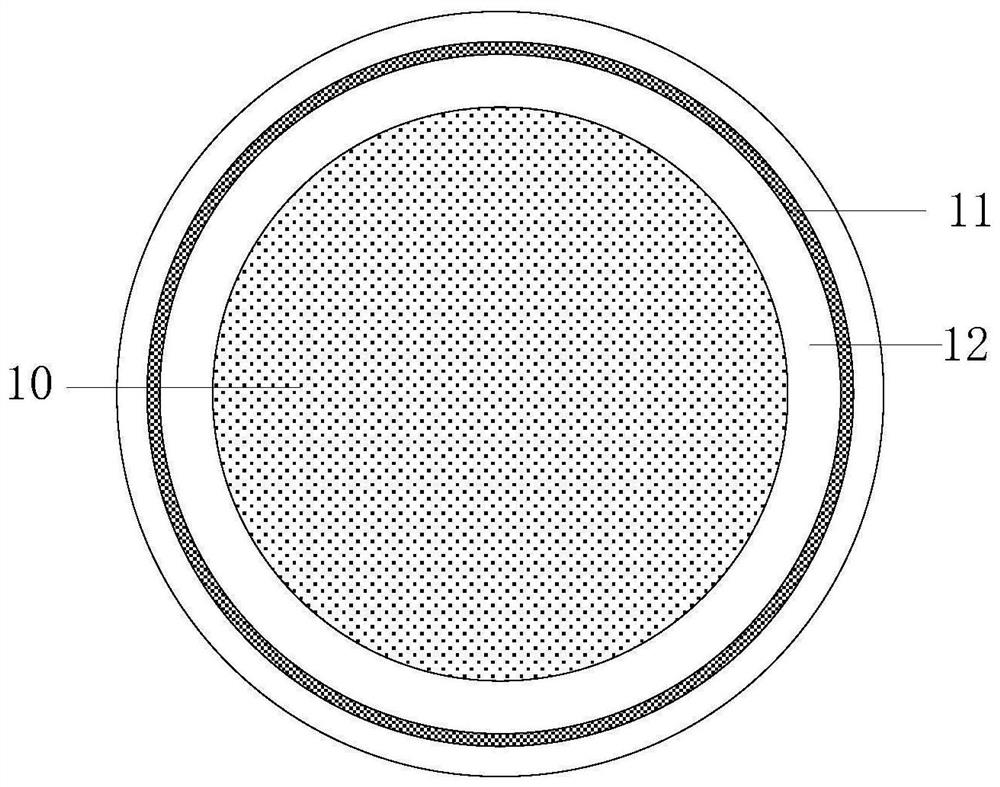
[0033] Based on this, the present invention provides a thin film growth assembly to overcome the above-mentioned problems in the prior art, including a target and a protective cover, the protective cover is detachably mounted on the target, and the protective cover A closed cavity is formed with the target, so as to seal the sputtering surface of the target in the closed cavity.

[0034] The thin film growth component, method and LED preparation method provided by th...


PUM


Abstract

The invention provides a thin film growth assembly and method and an LED fabrication method. The thin film growth assembly comprises a target material and a protection cover, wherein the protection cover is detachably arranged on the target material, and the protection cover and the target material form a closed cavity so that a sputtering surface of the target material is sealed in the closed cavity. In the thin film growth assembly, an AlGaN thin film is grown under N2 atmosphere by an AlGa alloy target material and is used as a buffer layer of the LED device; and compared with an ALN bufferlayer, the AlGaN buffer layer fabricated on a substrate surface by the AlGa alloy target has the advantages that the lattice stress of the subsequently-formed GaN thin film can be effectively improved, and the performance of the LED device is improved.

Description

technical field [0001] The invention relates to the technical field of semiconductors, in particular to a thin film growth component, method and LED preparation method. Background technique [0002] In the LED field, adding an AlN buffer layer on the substrate can effectively improve the photoelectric performance and equipment productivity of LED devices, and reduce production costs. In the prior art, magnetron sputtering is mostly used to prepare a high-quality AlN buffer layer with a target thickness on the substrate. [0003] Magnetron sputtering is a physical vapor deposition process, which uses high-energy ions to hit the surface of a solid target to cause sputtering of the target, and deposits the sputtered particles on the surface of the substrate to form a thin film. In the prior art, when the AlN buffer layer of the GaN-based epitaxial material is prepared by the magnetron sputtering process, the pure aluminum target is generally used for sputtering, and the N 2 T...

Claims


Application Information

Patent Timeline
Patent Type & Authority Patents(China)
IPC IPC(8): H01L33/00H01L33/32
CPCH01L33/0075H01L33/32
Inventor 王爱民程伟尧刚卓祥景
Owner XIAMEN CHANGELIGHT CO LTD
Features
  • R&D
  • Intellectual Property
  • Life Sciences
  • Materials
  • Tech Scout
  • Unparalleled Data Quality
  • Higher Quality Content
  • 60% Fewer Hallucinations
Learn More