
A kind of LED structure and manufacturing method thereof

A technology of LED structure and manufacturing method, which is applied in the direction of semiconductor devices, electrical components, circuits, etc., can solve the problems of reduced photoelectric performance of LED devices, residual aluminum, and affecting the quality of epitaxial structure crystals, etc., to achieve luminous performance improvement and lattice stress. Small, small Stark effect

Active Publication Date: 2021-02-02
XIAMEN CHANGELIGHT CO LTD
View PDF5 Cites 0 Cited by
  • Summary
  • Abstract
  • Description
  • Claims
  • Application Information

AI Technical Summary

Problems solved by technology

[0006] In order to solve the above-mentioned technical problems, the embodiment of the present invention provides an LED structure and its manufacturing method to solve the problem that in the existing LED manufacturing method, after the formation of the aluminum nitride buffer layer, there are still many aluminum residues in the reaction chamber. , affecting the crystal quality of the subsequently formed epitaxial structure, leading to the problem that the optoelectronic performance of the LED device is reduced

Method used


Image

  • A kind of LED structure and manufacturing method thereof
  • A kind of LED structure and manufacturing method thereof
  • A kind of LED structure and manufacturing method thereof

Examples


Embodiment Construction

[0037] The following will clearly and completely describe the technical solutions in the embodiments of the present invention with reference to the accompanying drawings in the embodiments of the present invention. Obviously, the described embodiments are only some, not all, embodiments of the present invention. Based on the embodiments of the present invention, all other embodiments obtained by persons of ordinary skill in the art without making creative efforts belong to the protection scope of the present invention.

[0038] In the following description, a lot of specific details are set forth in order to fully understand the present invention, but the present invention can also be implemented in other ways different from those described here, and those skilled in the art can do it without departing from the meaning of the present invention. By analogy, the present invention is therefore not limited to the specific examples disclosed below.

[0039] As mentioned in the back...


PUM

PropertyMeasurementUnit
thicknessaaaaaaaaaa

Abstract

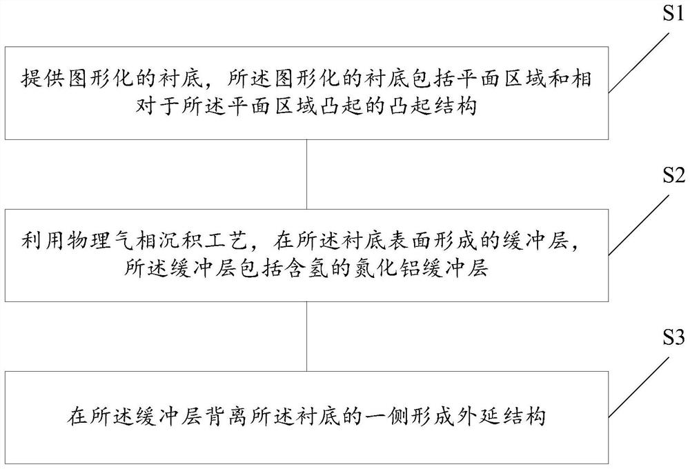
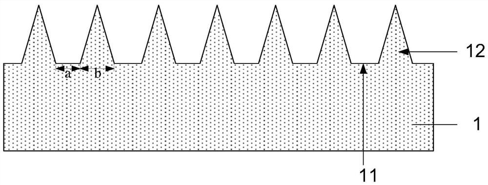
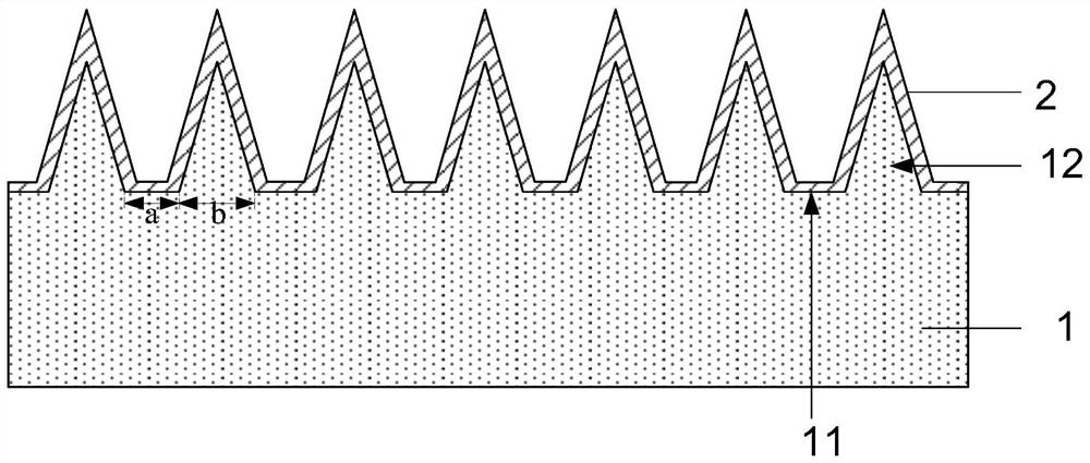
The embodiment of the invention discloses an LED structure and a manufacturing method thereof. The method includes the following steps: providing a graphical substrate; forming a buffer layer on the surface of the substrate by using a physical vapor deposition process, wherein the buffer layer includes a hydrogen-containing aluminum nitride buffer layer; and forming an epitaxial structure on one side of the buffer layer facing away from the substrate. Thereby, the problem that in an existing LED structure manufacturing method, after the aluminum nitride buffer layer is formed, many aluminum residues still exist in a reaction chamber, the crystal quality of the subsequently formed epitaxial structure is affected, and the photoelectric performance of an LED device is reduced can be solved; the lattice stress between the substrate and the epitaxial structure can also be improved, so that the surface temperature field of the epitaxial structure of an LED can be uniform, the uniformity of the wavelength of the light emitted by the LED structure can be greatly improved, and meanwhile, the quantum-confined Stark effect on quantum wells can be reduced, so that the luminous performance of the finally formed LED can be improved, the brightness can be increased, and the leakage current can be reduced.

Description

technical field [0001] The invention relates to the technical field of LED manufacturing, in particular to an LED structure and a manufacturing method thereof. Background technique [0002] LED is called the fourth-generation lighting source or green light source. It has the characteristics of energy saving, environmental protection, long life, and small size. It is widely used in various indications, displays, decorations, backlights, general lighting, and urban night scenes. [0003] In the current LED manufacturing process, usually before forming an epitaxial structure on the substrate, an aluminum nitride buffer layer is formed on the surface of the substrate to improve the photoelectric performance of the LED device, increase the production capacity of the LED device, and reduce the cost. [0004] The existing method of forming an aluminum nitride buffer layer on a substrate usually uses an organic chemical vapor deposition process to form an aluminum nitride buffer lay...

Claims


Application Information

Patent Timeline
Patent Type & Authority Patents(China)
IPC IPC(8): H01L33/00H01L33/12
CPCH01L33/007H01L33/12
Inventor 王爱民程伟尧刚崔晓慧
Owner XIAMEN CHANGELIGHT CO LTD
Learn More