Semiconductor wafer scribing device and method

A semiconductor and wafer technology, which is applied in the field of semiconductor wafer dicing devices, can solve problems such as long process time and achieve the effect of improving efficiency

Pending Publication Date: 2019-08-30
FUJIAN PRIMA OPTOELECTRONICS CO LTD
View PDF0 Cites 0 Cited by
  • Summary
  • Abstract
  • Description
  • Claims
  • Application Information

AI Technical Summary

Problems solved by technology

[0005] As mentioned above, the conventional device that scribbles sequentially in the Y direction and the X direction has a process of rotating the wafer, so the process takes a long time.

Method used


Image

  • Semiconductor wafer scribing device and method
  • Semiconductor wafer scribing device and method
  • Semiconductor wafer scribing device and method

Examples


Embodiment Construction

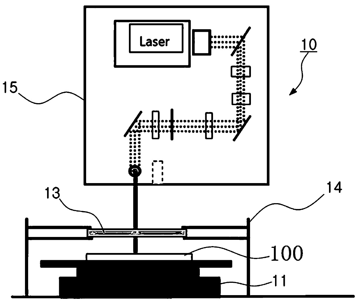
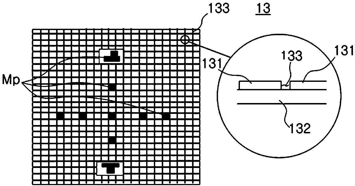
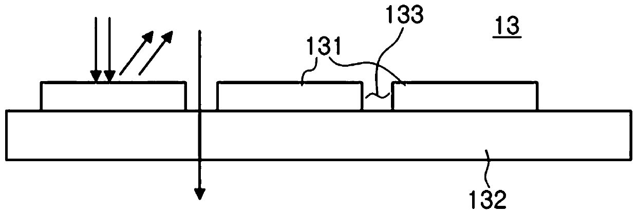
[0032] Such as Figure 1-6 As shown, the semiconductor wafer dicing device, the dicing device 10 includes a laser 15 and a wafer mold; Wafer carrier 11; the scribe mask includes a laser-permeable scribe area 133 and a blocking area 131 for laser blocking; the scribe area and the blocking area form a mask pattern; the mask The pattern includes the expected divided shape of the semiconductor wafer; when the wafer is divided, the laser of the laser passes through the scribed area of ​​the dicing mask, and the wafer on the wafer carrier is cut according to the mask pattern.

[0033] The blocking area uses a frequency doubling material to block laser light from the laser.

[0034] The wafer carrier is movable so that the semiconductor wafer it carries is aligned with the mask pattern of the dicing mask.

[0035] The dicing device also includes an image system, which is used to align the preset positioning points on the wafer with the pattern positioning points of the mask pattern...


PUM


Abstract

The invention provides a semiconductor wafer scribing device. The scribing device comprises a laser and a wafer die, wherein the wafer die includes a scribing mask, a wafer and a wafer bearing frame used for bearing the semiconductor wafer which are sequentially arranged in the laser incident direction; the scribing mask includes a scribing area capable of transmitting laser light and a blocking area capable of blocking the laser light; the scribing area and the blocking area form a mask pattern; the mask pattern includes an expected division shape of the semiconductor wafer; and the laser light of the laser passes through the scribing area of the scribing mask and cuts the wafer on the wafer bearing frame according to the mask pattern when the wafer is divided. The semiconductor wafer scribing efficiency can be improved according to the invention.

Description

technical field [0001] The invention relates to the technical field of semiconductor processing, in particular to a semiconductor wafer dicing device and a dicing method. Background technique [0002] The manufacture of semiconductors such as LEDs (Light Emitting Diodes, light emitting diodes) includes a process of forming multiple elements on a wafer at one time and then separating them into individual chips (die) and packaging them. The former is called the front-end process, and the latter is called the back-end process. It can be said that in terms of the quality of semiconductor elements, the front-end process of forming multiple elements on a wafer has a greater impact, but the importance of the back-end process is no less important than the former. [0003] In the back-end process, the process of separating the wafer into multiple elements (die) is called dicing, and dicing includes scribing and splitting or truncation of lines drawn with a laser on the surface of th...

Claims


Application Information

Patent Timeline
Patent Type & Authority Applications(China)
IPC IPC(8): H01L21/67H01L21/78B23K26/38
CPCB23K26/38H01L21/67092H01L21/78
Inventor 吴永胜林新汪雪琴
Owner FUJIAN PRIMA OPTOELECTRONICS CO LTD
Why Eureka
Try Eureka