
Super junction device structure and preparation method thereof

A super-junction device and column structure technology, applied in the field of super-junction device structure and its preparation, can solve problems such as difficult to meet the depth of p-column, achieve the effect of optimizing vertical electric field distribution, suitable for large-scale manufacturing, and improving withstand voltage characteristics

Inactive Publication Date: 2019-09-10
上海功成半导体科技有限公司
View PDF6 Cites 0 Cited by
  • Summary
  • Abstract
  • Description
  • Claims
  • Application Information

AI Technical Summary

Problems solved by technology

Existing etching and epitaxial filling processes have been difficult to meet the increasing p-pillar depth with product upgrades

Method used


Image

  • Super junction device structure and preparation method thereof
  • Super junction device structure and preparation method thereof
  • Super junction device structure and preparation method thereof

Examples


Embodiment 1

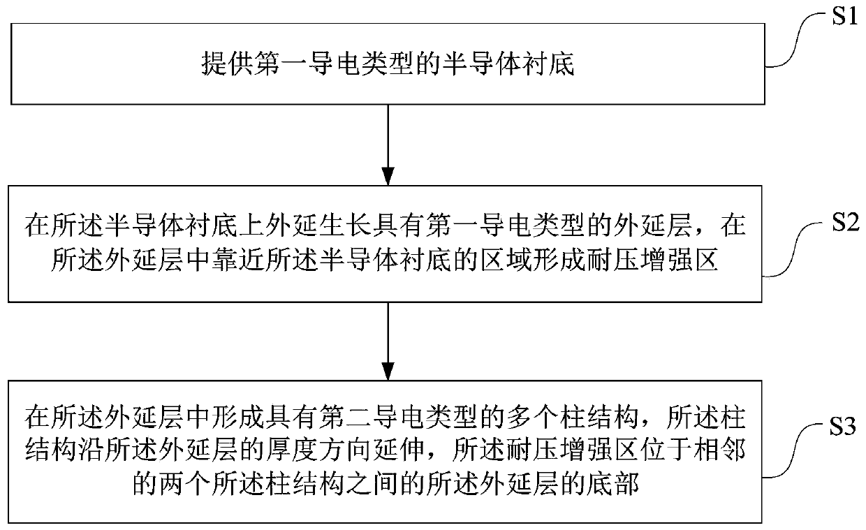
[0066] see Figure 1 to Figure 12 , the invention provides a method for preparing a superjunction device structure, comprising the following steps:

[0067] 1) providing a semiconductor substrate 101 of the first conductivity type;

[0068] 2) epitaxially growing an epitaxial layer 102 with a first conductivity type on the semiconductor substrate 101, and forming a withstand voltage enhanced region 103 in a region of the epitaxial layer 102 close to the semiconductor substrate 101

[0069] 3) Forming a plurality of pillar structures 104 with the second conductivity type in the epitaxial layer 102, the pillar structures 104 extending along the thickness direction of the epitaxial layer 102, and the withstand voltage enhanced regions 103 are located in two adjacent The lower part of the epitaxial layer 102 between the pillar structures 104.

[0070] In step 1), see figure 1 The S1 step and figure 2 , providing a semiconductor substrate 101 of the first conductivity type. fi...

Embodiment 2

[0109] This embodiment provides a super-junction device structure and its preparation method. Compared with the trench-type super-junction structure in Embodiment 1, the difference of this embodiment is that this embodiment adopts an epitaxial injection-type super-junction structure, so The pillar structure is formed by multiple epitaxy and implantation.

[0110] As an example, based on the lower epitaxial layer and the enhanced withstand voltage region formed in the first embodiment, when forming the upper epitaxial layer and a plurality of pillar structures with the second conductivity type, first epitaxially grow type of sub-epitaxial layer, and then perform ion implantation and annealing in the region where the column structure is located. After the superposition of multiple sub-epitaxial layers, the multiple sub-epitaxial layers form the upper epitaxial layer, and the implanted regions are aligned and superimposed to form the column structure.

[0111] Other compositions...


PUM

PropertyMeasurementUnit
Thicknessaaaaaaaaaa
Thicknessaaaaaaaaaa

Abstract

The invention provides a super junction device structure and a preparation method thereof. The super junction device structure includes a semiconductor substrate of a first conductivity type; an epitaxial layer of the first conductivity type formed on the semiconductor substrate, a plurality of column structures of a second conductivity type formed in the epitaxial layer, extending along the thickness direction of the epitaxial layer and arranged in the epitaxial layer in a direction parallel to the surface of the semiconductor substrate, and a voltage-withstanding enhancement region of the second conductivity type formed in the epitaxial layer and located below the epitaxial layer between two adjacent column structures. By forming the voltage-withstanding enhancement region below the epitaxial layer between the column structures, the longitudinal electric field distribution of the super junction device is optimized, and the voltage-withstanding characteristic of the super junction device is further improved without increasing the depth of the column structures. The preparation method provided by the invention has a simple preparation process and low cost, and is suitable for large-scale manufacturing.

Description

technical field [0001] The invention relates to the field of semiconductor integrated circuit manufacturing, in particular to a superjunction device structure and a preparation method thereof. Background technique [0002] Power devices play a pivotal role in the field of power electronics technology. Among them, the superjunction device (superjunction) has attracted much attention due to its extremely high withstand voltage capability and excellent conductivity, and the research and development of the superjunction device is becoming a hot spot in this field. [0003] At present, the high withstand voltage characteristics of super-junction power devices are one of the main directions of research and development of super-junction devices. When the super-junction device is in the off state, the lateral alternate p-regions and n-regions in the substrate form a depletion layer through the charge balance of the horizontal horizontal electric field, thereby realizing the high wi...

Claims


Application Information

Patent Timeline
IPC IPC(8): H01L29/06H01L29/78H01L21/336
CPCH01L29/0634H01L29/0623H01L29/7827H01L29/66666
Inventor 柴展罗杰馨薛忠营徐大朋
Owner 上海功成半导体科技有限公司
Learn More