Organic light-emitting electronic device packaging structure and production process thereof

A technology of organic electronic devices and organic light-emitting devices, which is applied in the field of electrical device processing, can solve problems such as light attenuation, achieve the effects of reducing light attenuation, improving packaging effects, and avoiding damage

Inactive Publication Date: 2019-09-17
FLEXIBLE JIANGSU MATERIALS CO LTD
View PDF3 Cites 2 Cited by
  • Summary
  • Abstract
  • Description
  • Claims
  • Application Information

AI Technical Summary

Problems solved by technology

In addition, since the device and each encapsulation layer are all light-transmitting materials, it is bound to cause UV to easily enter the organic device layer and cause light attenuation.

Method used


Image

  • Organic light-emitting electronic device packaging structure and production process thereof
  • Organic light-emitting electronic device packaging structure and production process thereof

Examples


Embodiment Construction

[0034] Specific embodiments of the present invention are described in detail below, but it should be understood that the protection scope of the present invention is not limited by the specific embodiments.

[0035] Unless expressly stated otherwise, throughout the specification and claims, the term "comprise" or variations thereof such as "includes" or "includes" and the like will be understood to include the stated elements or constituents, and not Other elements or other components are not excluded.

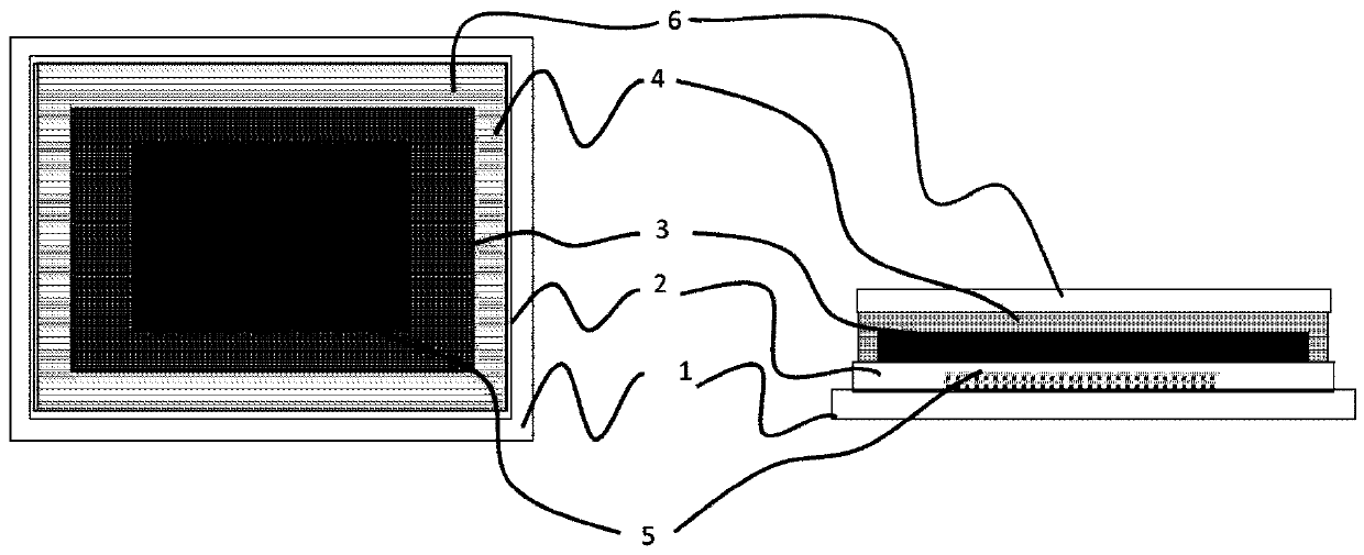
[0036] An organic light-emitting electronic device packaging structure, comprising: an organic electronic device or an organic functional layer prepared on a substrate, a protective insulating layer on the organic light-emitting device, a metal layer deposited on the protective insulating layer, and a metal layer on the metal layer UV curable organic layers, and upper encapsulation cover.

[0037]Wherein, the substrate is selected from metals, quartz, silicon oxide, glass, si...


PUM

PropertyMeasurementUnit
thicknessaaaaaaaaaa

Abstract

The design of a metal insertion layer is added in an organic light-emitting electronic device packaging layer, by the packaging technology of inserting a nano-scale metal nano-insertion layer and by using the light reflection and absorption of a dense metal nano film and the small size of metal atoms, most UV light can be reflected, and therefore, a fragile organic functional layer is protected. Secondly, when metal small molecules smaller than a nanometer scale and an underlying insulating layer form a dense water-oxygen molecular barrier layer, the packaging effect is further improved.

Description

[0001] Technical field: [0002] The invention belongs to the technical field of electrical device processing, and in particular relates to an organic light-emitting electronic device packaging structure and a packaging process thereof. [0003] Background technique: [0004] New organic electronic devices, organic light emitting devices, organic optoelectronic devices, organic detectors and organic field effect tubes are widely used in display and solid-state lighting, energy sources, detectors, mobile phones, wearables, etc. The field has broad application prospects. Its excellent characteristics will affect the development of next-generation display electronics, and it is the main force of flexible electronic displays. [0005] However, according to a long-term, a large number of organic electronics studies have shown that the water vapor and oxygen components in the air have a fatal impact on organic electronic devices. The main reason is that water vapor and oxygen molecu...

Claims


Application Information

Patent Timeline
Patent Type & Authority Applications(China)
IPC IPC(8): H01L51/52H01L51/56
CPCH10K50/8423H10K50/84H10K50/844H10K71/00
Inventor 林群
Owner FLEXIBLE JIANGSU MATERIALS CO LTD
Why Eureka
Try Eureka