Semiconductor device fault detecting method and device, and converter

A fault detection and semiconductor technology, applied in the field of power electronics, can solve the problems of high immunity, poor isolation, and no real-time performance, and achieve the effect of solving real-time performance

Pending Publication Date: 2019-09-20
SHENZHEN HOPEWIND ELECTRIC CO LTD
View PDF0 Cites 2 Cited by
  • Summary
  • Abstract
  • Description
  • Claims
  • Application Information

AI Technical Summary

Problems solved by technology

[0007] In view of this, the object of the present invention is to provide a semiconductor device fault detection method and device, converter, to solve the existing semiconductor device overcurrent, short circuit, direct detection does not have real-time, high immunity and isolation. bad question

Method used


Image

  • Semiconductor device fault detecting method and device, and converter
  • Semiconductor device fault detecting method and device, and converter
  • Semiconductor device fault detecting method and device, and converter

Examples


no. 1 example

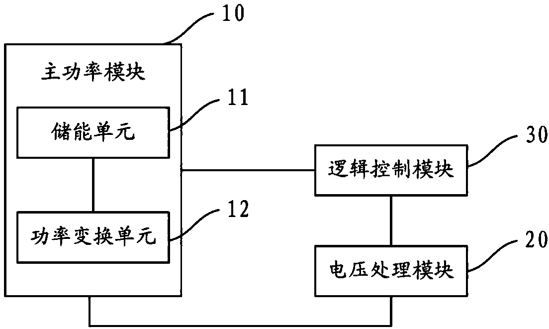
[0034] Such as figure 1 As shown, the first embodiment of the present invention provides a semiconductor device failure detection device, the device includes: a main power module 10, a voltage processing module 20, and a logic control module 30;

[0035] The main power module 10 includes an energy storage unit 11 and a power conversion unit 12, and the power conversion unit 12 includes a semiconductor device (not shown in the drawings).

[0036] In this embodiment, the power conversion unit 12 includes, but is not limited to, an "I" type three-level topology circuit, a "T" type three-level topology circuit, a "Vienna-Like" three-level topology circuit, and a two-level converter. Topological circuit, energy discharge topological circuit, etc. The number of power conversion units 12 is not limited here.

[0037] The voltage processing module 20 is configured to collect the voltage between the preset nodes of the power conversion unit 12; convert the voltage between the preset nodes in...

no. 2 example

[0072] Such as Figure 7 As shown, the second embodiment of the present invention provides a semiconductor device failure detection method, and the method includes the steps:

[0073] S11. Collect voltages between preset nodes of the power conversion unit.

[0074] Please refer to Picture 10 As shown, taking the "I" type three-level topology circuit as an example, the preset nodes can be the midpoint N on the DC side and the midpoint L on the power conversion side in the power conversion unit 12. By collecting the data between N and L Voltage to determine whether the semiconductor device fails. In practical applications, including but not limited to the voltage between these two points.

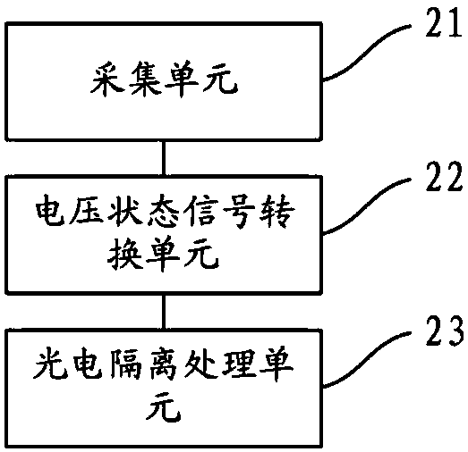
[0075] S12: Convert the voltage between the preset nodes into a voltage state signal.

[0076] Please refer to Figure 8 As shown, in this embodiment, the converting the voltage between the preset nodes into a voltage state signal includes the steps:

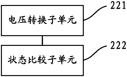
[0077] S121: Converting the voltage of the volt...

no. 3 example

[0096] The third embodiment of the present invention provides a converter including the semiconductor device failure detection apparatus described in the first embodiment. The semiconductor device failure detection device can refer to the foregoing content, which will not be repeated here.

[0097] The converter of the embodiment of the present invention converts the collected voltage into a voltage state signal, outputs a low-voltage signal after isolation processing, and compares the low-voltage signal with the drive control signal to determine whether a semiconductor device fails, and can detect semiconductor device failures in real time , It solves the problems that the existing semiconductor device failure detection does not have real-time performance, high immunity and poor isolation.

[0098] It should be noted that the foregoing device embodiment and method embodiment belong to the same concept. For the specific implementation process, refer to the method embodiment, and th...


PUM


Abstract

The invention discloses a semiconductor device fault detecting method and device, and a converter. The device comprises a main power module, a voltage processing module and a logic control module. The main power module comprises an energy storage unit and a power conversion unit. The power conversion unit comprises a semiconductor device. The voltage processing module is used to collect a voltage between preset nodes of the power conversion unit. The voltage between the preset nodes is converted into a voltage state signal. Photoelectric isolation processing is performed on the voltage state signal and then a low voltage signal is output. The logic control module is used to obtain the low voltage signal output by the voltage processing module. Whether the semiconductor device has a fault is determined according to a driving control signal of the power conversion unit and the low voltage signal. In the invention, the fault of the semiconductor device can be detected in real time, and problems that detection of an existing semiconductor device fault does not have real-time performance and high disturbance rejection performance, and has poor isolation performance are solved.

Description

Technical field [0001] The present invention relates to the technical field of power electronics, in particular to a method and device for detecting faults of semiconductor devices, and a converter. Background technique [0002] Semiconductor devices are the core components of the power conversion unit. After a failure, the voltage at both ends of the semiconductor device will change, which will cause the voltage state of the key nodes of the power conversion unit to also change. On the other hand, before the failure of the semiconductor device, Its own characteristics will produce abnormalities, causing the voltage at both ends to be different from the voltage during normal operation, and will also cause changes in the voltage state of the key nodes of the power conversion unit. By detecting the voltage state at both ends of the key nodes in the power conversion unit, it can be determined whether the semiconductor in the power conversion unit is abnormal. After the abnormality ...

Claims


Application Information

Patent Timeline
Patent Type & Authority Applications(China)
IPC IPC(8): G01R31/26
CPCG01R31/2601
Inventor 李海龙王武华霍明郑大鹏周党生
Owner SHENZHEN HOPEWIND ELECTRIC CO LTD
Why Eureka
Try Eureka