Lead-free integrated circuit chip packaging structure

A chip packaging structure and integrated circuit technology, applied in the direction of circuits, electrical components, electric solid devices, etc., can solve the problems affecting the stability of pin connection, moisture adhesion on pins, etc., and achieve good moisture resistance and dustproof effect , the effect of preventing short circuit

Active Publication Date: 2019-09-20
南通优睿半导体有限公司
View PDF4 Cites 4 Cited by
  • Summary
  • Abstract
  • Description
  • Claims
  • Application Information

AI Technical Summary

Problems solved by technology

[0003] Aiming at the deficiencies of the prior art, the present invention provides a leadless integrated circuit chip packaging structure, which has the advantages of preventing the surface of the pins and protecting the connection betwee

Method used


Image

  • Lead-free integrated circuit chip packaging structure
  • Lead-free integrated circuit chip packaging structure
  • Lead-free integrated circuit chip packaging structure

Examples


Embodiment Construction

[0016] The following will clearly and completely describe the technical solutions in the embodiments of the present invention with reference to the accompanying drawings in the embodiments of the present invention. Obviously, the described embodiments are only some, not all, embodiments of the present invention. Based on the embodiments of the present invention, all other embodiments obtained by persons of ordinary skill in the art without making creative efforts belong to the protection scope of the present invention.

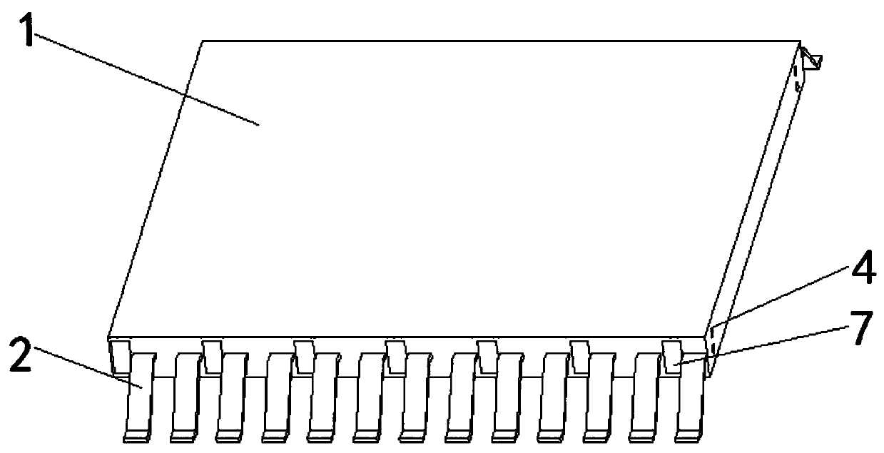
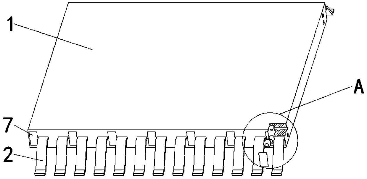
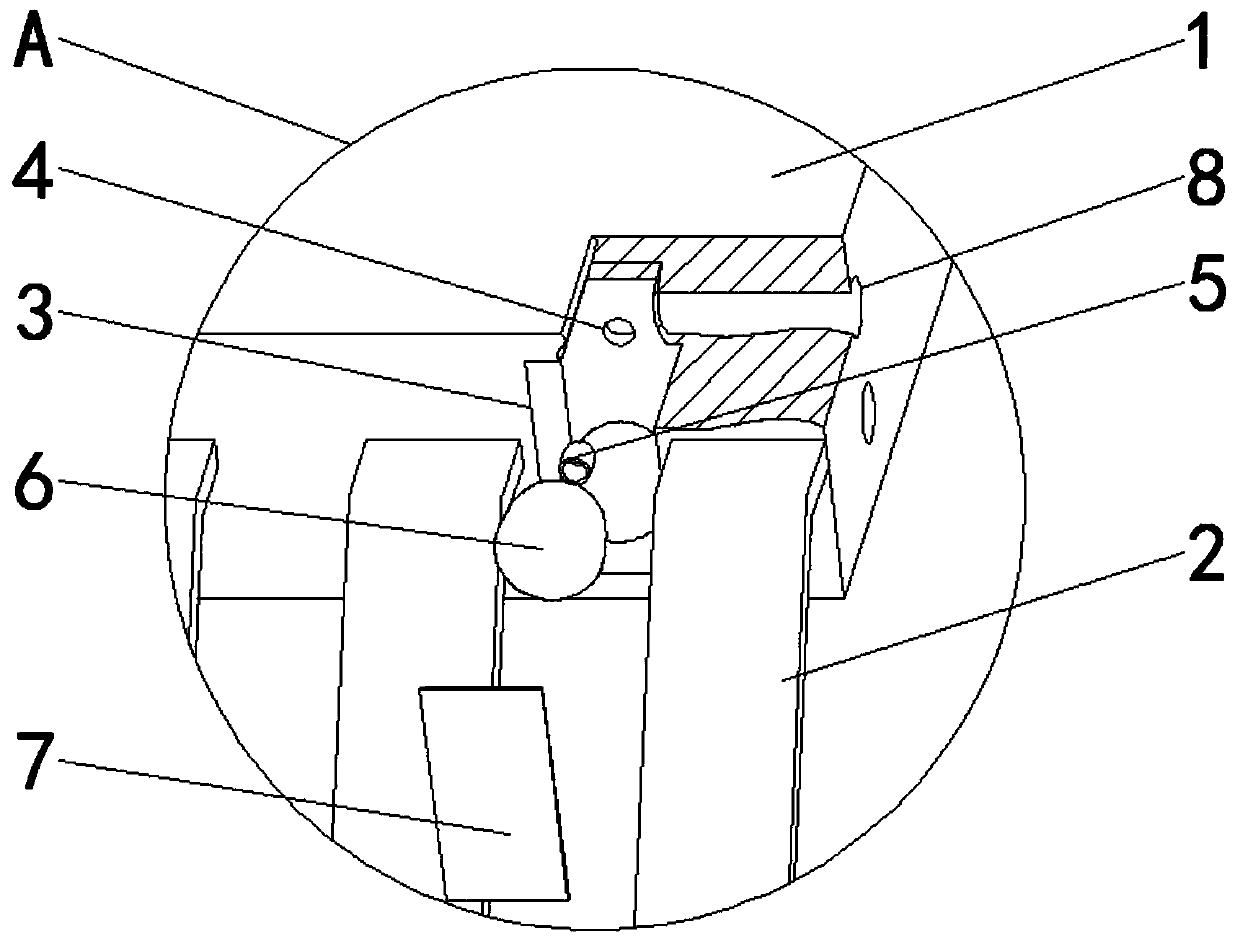
[0017] see Figure 1-3 , a leadless integrated circuit chip packaging structure, including a chip package 1 and pins 2, the number of pins 2 is twenty-six, which can be determined according to actual conditions, and the pins 2 are fixedly mounted on the chip package 1 The front and rear sides of the chip package 1 are provided with safety slots 3, the number of safety slots 3 is fourteen, and each safety slot 3 is located between two corresponding pins 2 In b...


PUM


Abstract

The invention relates to the technical field of a packaging structure, and discloses a lead-free integrated circuit chip packaging structure. The lead-free integrated circuit chip packaging structure comprises a chip packaging body and pins, wherein the number of the pins is twenty-six, the pins are fixedly installed on the front and rear sides of the chip packaging body, both the front and rear sides of the packaging body are provided with safety slots, the number of the safety slots is fourteen, each safety slot is located between the corresponding two pins, the rear side in each safety slot is provided with an inflation hole, and the internal part of each inflation hole is fixedly sleeved with an inflation connector. The lead-free integrated circuit chip packaging structure ensures that there will be no short circuit due to moisture during the operation process through protecting the pins. Meanwhile, rubber has insulation and can prevent a short circuit caused by static electricity generated between the two pins, and the wrapping of an air bag can have an excellent dustproof effect.

Description

technical field [0001] The invention relates to the technical field of package structures, in particular to a leadless integrated circuit chip package structure. Background technique [0002] The packaging of integrated circuit chips refers to the housing used to install semiconductor integrated circuit chips. It plays the role of placing, fixing, sealing, protecting the chips and enhancing the electrothermal performance. To establish a connection, that is to solder the pins on the circuit board, but because each circuit board has different requirements for the length of the pin welding, it is necessary to reserve a longer pin, so on the circuit board with a shorter pin requirement, it will cause The pins are exposed to the air. When working in a humid environment, the moisture in the air will adhere to the pins, causing the pins to short circuit and the chip to burn. At the same time, if the pins are too long, the chip will be suspended. When the circuit board is vibrated,...

Claims


Application Information

Patent Timeline
IPC IPC(8): H01L23/00H01L23/12H01L23/60
CPCH01L23/12H01L23/562H01L23/564H01L23/60
Inventor 不公告发明人
Owner 南通优睿半导体有限公司
Why Eureka
Try Eureka