Package structure of power device and manufacturing method of package structure
A packaging structure and power device technology, applied in semiconductor/solid-state device manufacturing, electric solid-state devices, semiconductor devices, etc., can solve problems affecting the height of sub-modules, achieve good heat dissipation advantages, realize double-sided heat dissipation, and eliminate chip pressure bad effect
- Summary
- Abstract
- Description
- Claims
- Application Information
AI Technical Summary
Problems solved by technology
Method used
Image

Examples
Embodiment Construction
[0034] The specific implementation manner of the present invention will be described in detail below in conjunction with the accompanying drawings.
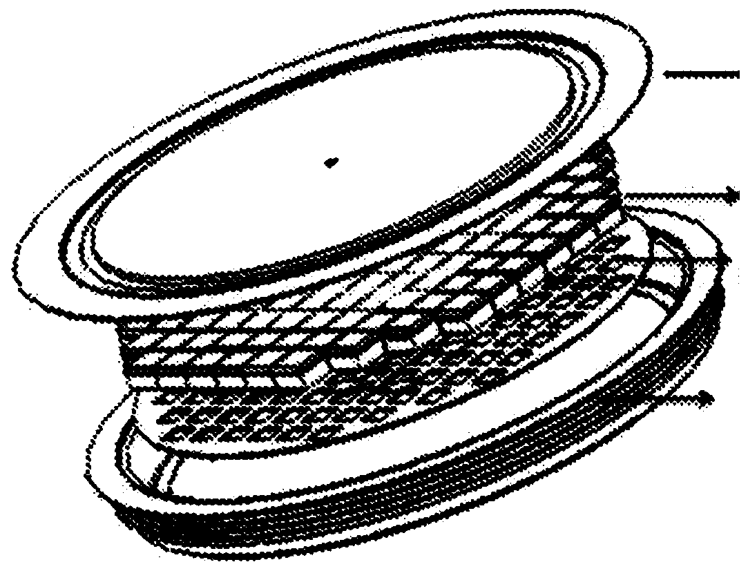
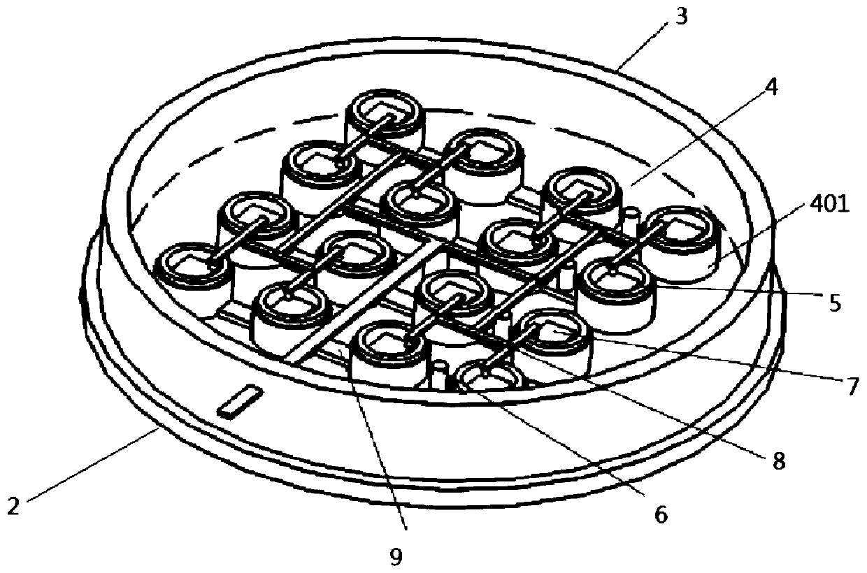
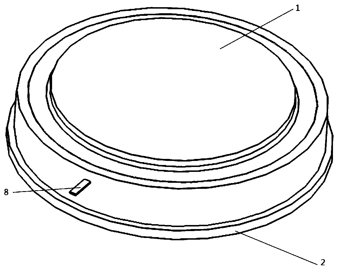
[0035] In a preferred embodiment, as figure 2 and image 3 As shown, the present invention provides a liquid metal-based power device packaging structure, including an upper end cover 1, a lower end cover 2, an insulating case 3, a base array 4, a sealing case 5, a liquid metal 6, an IGBT subunit 7, and a gate lead Frame 8 and Unicom groove 9.
[0036]The upper end cover 1 and the lower end cover 2 are two metal cover plates, which serve as the power end of the packaging structure and sandwich the insulating shell 3 in between to form a cavity. In the cavity, a plurality of bases 401 are formed on the lower cover plate 2, wherein the bases 401 having the same number as the required IGBT subunits communicate with each other through the communication groove 9, and multiple groups of interconnected bases 401 are arranged side by ...
PUM
 Abstract
Description
Claims
Application Information
 - R&D
- Intellectual Property
- Life Sciences
- Materials
- Tech Scout
- Unparalleled Data Quality
- Higher Quality Content
- 60% Fewer Hallucinations
Browse by: Latest US Patents, China's latest patents, Technical Efficacy Thesaurus, Application Domain, Technology Topic, Popular Technical Reports.
© 2025 PatSnap. All rights reserved.Legal|Privacy policy|Modern Slavery Act Transparency Statement|Sitemap|About US| Contact US: help@patsnap.com