
Eureka
For R&D, Eureka makes reading and utilizing patents & technical documents easy.
Eureka AIR
Designed for self-driven R&D workflows. Generate viable solutions, solve complex R&D challenges, empower your innovation with AI.

Eureka Materials
Designed for material experts only. Revolutionize your material R&D, from search, analyze, to developing new materials.

TechResearch
Generate reliable direction feasibility study reports for your R&D in just a few steps.

TechSeek
Discover and master advanced knowledge NOW. Basics, ideas, possibilities, all at once.

TechMind
As an expert in R&D Theories, TechMind can generates customized viable solutions instantly.

TechRisk
Analyze your overall solution with one click, know your potential R&D risks in advance.

TechMonitor
Get weekly tech updates, stay abreast of the latest tech innovations and key insights.
Photoelectric detector
A photodetector and electrode technology, applied in the field of photodetectors, can solve problems such as increased difficulty
- Summary
- Abstract
- Description
- Claims
- Application Information
AI Technical Summary
Problems solved by technology
Method used
Image

Examples
Embodiment 1
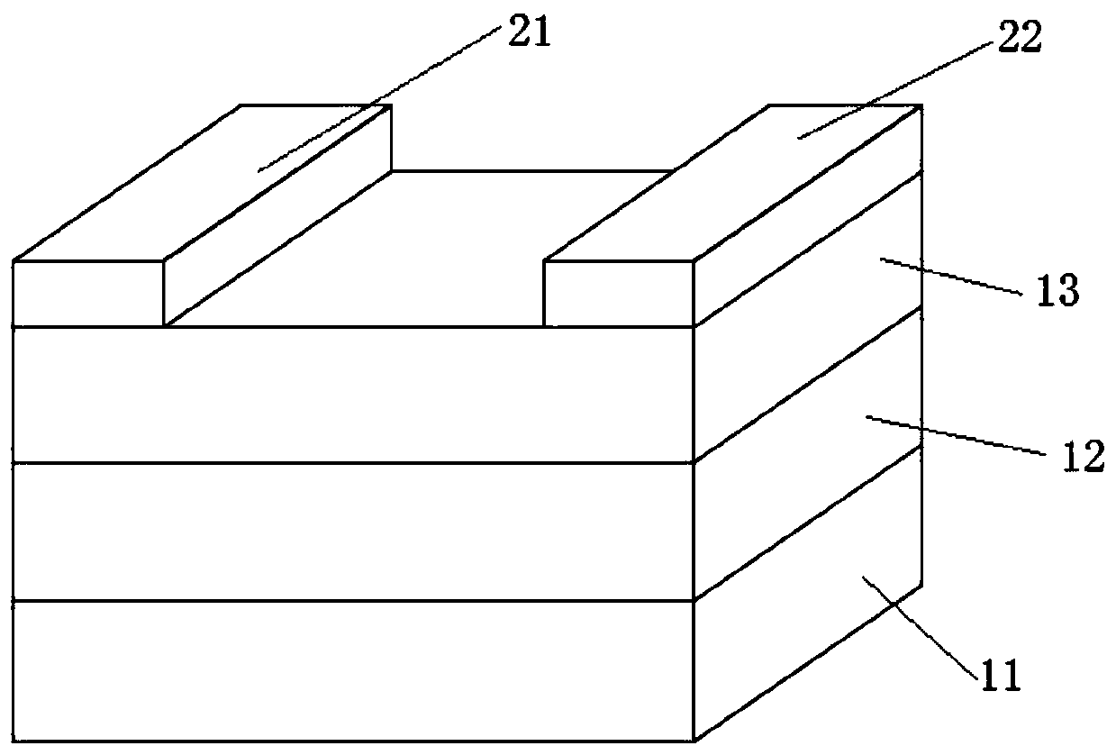
[0031] An embodiment of the present invention provides a photodetector, such as figure 1 As shown, it includes an absorber and an electrode layer, wherein the absorber includes a substrate layer 11, a reflective layer 12, and an absorbing layer 13 from bottom to top, and the electrode layer includes a first electrode 21 and a second electrode 22, so Both the first electrode 21 and the second electrode 22 are disposed on the absorption layer 13 .
[0032] Here, the material of the substrate layer 11 is generally silicon oxide.
[0033] The reflective layer 12 is grown on the substrate layer 11 by ion sputtering or template removal method, and the material of the reflective layer 12 is gold or silver. Specifically, when used, the thickness of the reflective layer 12 is 50 ~100nm. In this way, the thickness of the reflective layer is large enough to reflect all the light, so that it continues to propagate in the absorbing layer and gradually attenuates.
[0034] The absorbing ...
Embodiment 2
[0046] Specifically, the preparation method of the photodetector includes:
[0047] Step 1: providing the substrate layer made of silicon oxide;
[0048] Step 2: growing a reflective layer made of gold on the substrate layer by ion sputtering, with a thickness of 50 nm;
[0049] Step 3: 1 g of ethylenediaminetetraacetic acid (EDTA) and 1 g of polyethyleneimine (PEI) were mixed and dissolved in 30 mL of deionized water to form a solution;
[0050] Step 4: in described solution, add 2g ammonium molybdate ((NH 4 ) 6 Mo 7 o 24 4H 2 O) forming a homogeneous polymer precursor;
[0051] Step 5: Stir the homogeneous polymer precursor and perform ultrafiltration, the molecular weight is less than 10000g mol -1 ;
[0052] Step 6: spin-coat the obtained precursor solution on the reflective layer to obtain a film containing molybdenum, the spin-coating speed is 8000rpm, and the spin-coating time is 30s;
[0053]Step 7: Put the film into the center of the quartz tube in the tube f...
Embodiment 3
[0061] Further, compared with Example 2, in this Example 3, the parameter settings in step 2 are modified. Specifically, a layer of the reflective layer made of silver is grown on the substrate layer by ion sputtering, and the thickness is 50nm.
PUM
 Abstract
Description
Claims
Application Information
 - R&D Engineer
- R&D Manager
- IP Professional
- Industry Leading Data Capabilities
- Powerful AI technology
- Patent DNA Extraction
Browse by: Latest US Patents, China's latest patents, Technical Efficacy Thesaurus, Application Domain, Technology Topic, Popular Technical Reports.
© 2024 PatSnap. All rights reserved.Legal|Privacy policy|Modern Slavery Act Transparency Statement|Sitemap|About US| Contact US: help@patsnap.com