Display panel

A technology for display panels and substrates, applied in static indicators, instruments, semiconductor devices, etc., can solve problems such as crosstalk, and achieve the effect of improving the phenomenon of crosstalk

Active Publication Date: 2019-10-01
KUNSHAN GO VISIONOX OPTO ELECTRONICS CO LTD
View PDF9 Cites 17 Cited by
  • Summary
  • Abstract
  • Description
  • Claims
  • Application Information

AI Technical Summary

Problems solved by technology

The voltage change on the data line will be coupled to the gate of the drive transistor, which will cause crosstalk

Method used


Image

  • Display panel
  • Display panel
  • Display panel

Examples


Embodiment Construction

[0027] The following will clearly and completely describe the technical solutions in the embodiments of the present application with reference to the drawings in the embodiments of the present application. Obviously, the described embodiments are only some of the embodiments of the present application, not all of them. Based on the embodiments in this application, all other embodiments obtained by persons of ordinary skill in the art without making creative efforts belong to the scope of protection of this application.

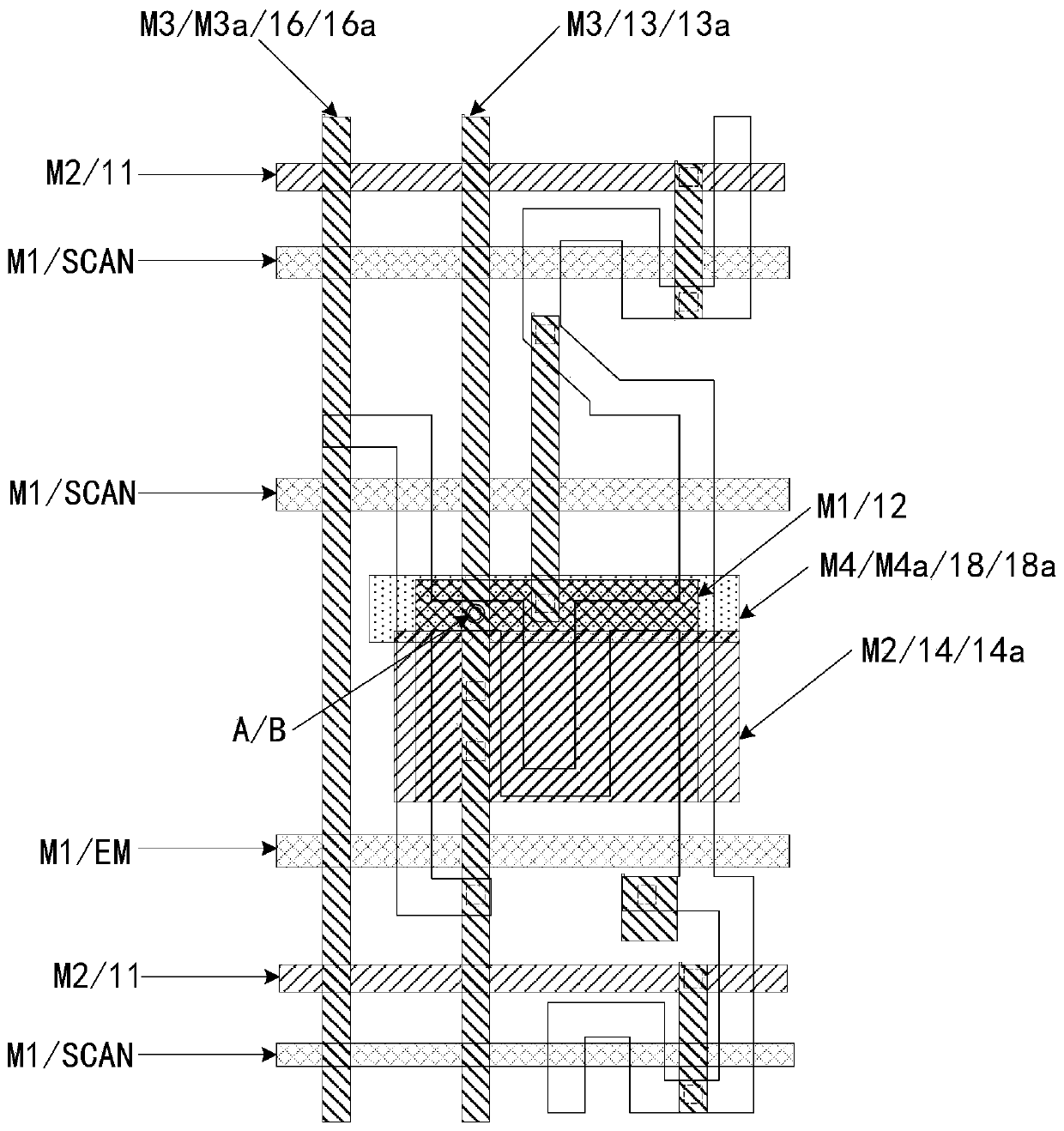
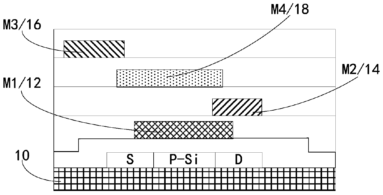
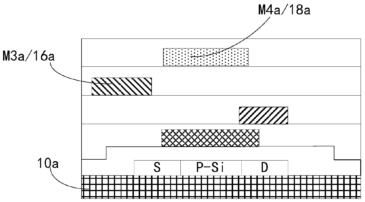
[0028] see Figure 1-Figure 2 , figure 1 It is a schematic plan view of an embodiment of the display panel of the present application, figure 2 for figure 1 A schematic cross-sectional view of an embodiment of the middle display panel. The display panel includes a substrate 10 ( figure 1 not shown), the first metal layer M1 , the second metal layer M2 , the third metal layer M3 and the first shielding electrode 18 .

[0029] Specifically, the substrate 1...


PUM


Abstract

The invention discloses a display panel which comprises a substrate, a first metal layer which is on a side of the substrate and includes a gate of a driving transistor, a second metal layer which ison a side of the first metal layer away from the substrate and includes a first base plate of a storage capacitor, a third metal layer which is on a side of the second metal layer away from the substrate and includes a data line, and a first shielding electrode which has a fixed potential, wherein an orthographic projection of the first base plate on the substrate partially coincides with an orthographic portion of the gate on the substrate, an orthographic projection of the data line on the substrate does not coincide with an orthographic projection of the gate on the substrate, and an orthographic projection of the gate on the substrate is in orthographic projections of the first shielding electrode and the first base plate on the substrate. In the above manner, the coupling capacitancebetween the gate of the driving transistor and the data line can be reduced, and therefore, the crosstalk phenomenon is reduced.

Description

technical field [0001] The present application relates to the field of display technology, in particular to a display panel. Background technique [0002] For an OLED (Organic Light Emitting Diode) display panel, the gate potential of the drive transistor determines the gray scale displayed. There is no overlapping capacitance between the gate of the driving transistor and the data line, but the lateral parasitic capacitance between them is unavoidable. With the improvement of the resolution of the display panel, the pixel layout space becomes smaller and smaller, and the parasitic capacitance between the gate of the driving transistor and the data line becomes larger and larger. The voltage change on the data line will be coupled to the gate of the driving transistor, thereby causing crosstalk. [0003] Therefore, under the development trend of further improving the resolution of the display panel, the phenomenon of crosstalk between the gate of the driving transistor and...

Claims


Application Information

Patent Timeline
Patent Type & Authority Applications(China)
IPC IPC(8): H01L27/32
CPCH10K59/12H10K59/131H10K59/126G09G3/3225G09G2320/0214
Inventor 贾溪洋吴剑龙朱正勇
Owner KUNSHAN GO VISIONOX OPTO ELECTRONICS CO LTD
Why Eureka
Try Eureka