High-power semiconductor device having failure open-circuit feature

A high-power, semiconductor technology, used in semiconductor devices, semiconductor/solid-state device components, electrical solid-state devices, etc., can solve problems such as electrical fire, drive load damage, motor burnout, etc., achieving high safety, practicability, The effect of avoiding short-circuit failure modes

Pending Publication Date: 2019-10-08
捷捷半导体有限公司
View PDF0 Cites 2 Cited by
  • Summary
  • Abstract
  • Description
  • Claims
  • Application Information

AI Technical Summary

Problems solved by technology

The final failure phenomenon is short-circuit failure, which will cause damage to the driving load (such as motor burnout), paralysis of the power grid system, and even serious problems such as electrical fires.

Method used


Image

  • High-power semiconductor device having failure open-circuit feature
  • High-power semiconductor device having failure open-circuit feature
  • High-power semiconductor device having failure open-circuit feature

Examples


Embodiment Construction

[0026] The following will clearly and completely describe the technical solutions in the embodiments of the present invention with reference to the accompanying drawings in the embodiments of the present invention. Obviously, the described embodiments are only some, not all, embodiments of the present invention. Based on the embodiments of the present invention, all other embodiments obtained by persons of ordinary skill in the art without making creative efforts belong to the protection scope of the present invention.

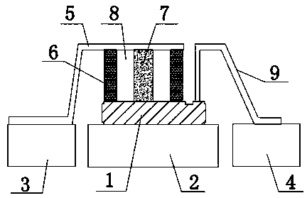
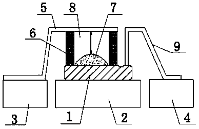
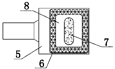
[0027] Examples, see Figure 1-4 , the present invention provides a technical solution: a high-power semiconductor device with failure open circuit characteristics, including a three-terminal high-power chip 1, an anode outer lead 2, a cathode outer lead 3, a control pole outer lead 4, and a cathode inner lead 5 , control electrode inner lead 9, insulating liner 6, low-temperature columnar conductive welding material 7, and air gap 8 between the insulating lin...


PUM


Abstract

The present invention relates to the technical field of power electronic devices and discloses a high-power semiconductor device having a failure open-circuit feature. The high-power semiconductor device comprises a three-terminal high-power chip, an anode external lead, a cathode external lead, a control electrode external lead, a cathode internal lead,, a control electrode internal lead, an insulating gasket, a low-temperature columnar conductive solder material, and an air gap between the insulating gasket and the columnar conductive solder material, wherein the insulating gasket is prefabricated on the cathode internal lead. When the high-power semiconductor device has a failure or is in a failure process caused by a fault, the temperature of the device rises sharply. When the temperature rises to the melting point of the prefabricated low-temperature columnar conductive solder material, the solder material melts and fills the air gap and causes a short circuit between the cathodeinternal lead and a chip, thereby causing a failure of the device or an open circuit before the failure and thus protecting the drive circuit of the device.

Description

technical field [0001] The invention relates to the technical field of power electronic devices, in particular to a high-power semiconductor device with a failure open circuit feature. Background technique [0002] Power semiconductor devices, also known as power electronic devices, are mainly used for high-power electronic devices in power conversion and control circuits of power equipment. Power devices include power diodes, thyristors, GTR, GTO, power MOSFETs, and IGBTs. [0003] In practical applications, if a load short-circuit fault occurs, excessive current will flow through the power device chip until overheating and failure, which is one of the common failure modes of power semiconductor devices. The final failure phenomenon is short-circuit failure, which will cause damage to the driving load (such as motor burnout), paralysis of the power grid system, and even serious problems such as electrical fires. [0004] Therefore, there needs to be the ability to shut off...

Claims


Application Information

Patent Timeline
Patent Type & Authority Applications(China)
IPC IPC(8): H01L23/62H01L23/488
CPCH01L23/62H01L23/488H01L2224/40245
Inventor 王成森吴家健
Owner 捷捷半导体有限公司
Why Eureka
Try Eureka