Resistive memory and making method thereof

A technology of resistive memory and manufacturing method, applied in the direction of electrical components, etc., can solve problems such as inability to provide low-power solutions, unfavorable low-voltage operation, etc.

Inactive Publication Date: 2019-10-08
MACRONIX INT CO LTD
View PDF4 Cites 0 Cited by
  • Summary
  • Abstract
  • Description
  • Claims
  • Application Information

AI Technical Summary

Problems solved by technology

[0004] However, typical resistive memory elements usually have a higher forming voltage than the operating voltage, which is not conducive to low-voltage operation, and cannot provide a low-power solution for electronic devices that require low-voltage operation, such as the Internet of Things (Internet of Things, IoT), wearable devices or portable electronic devices, such as laptops, tablets, smart watches, mobile phones, etc., to increase battery life

Method used


Image

  • Resistive memory and making method thereof
  • Resistive memory and making method thereof
  • Resistive memory and making method thereof

Examples


Embodiment Construction

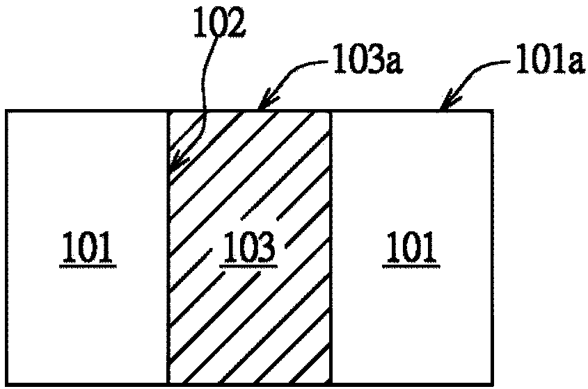
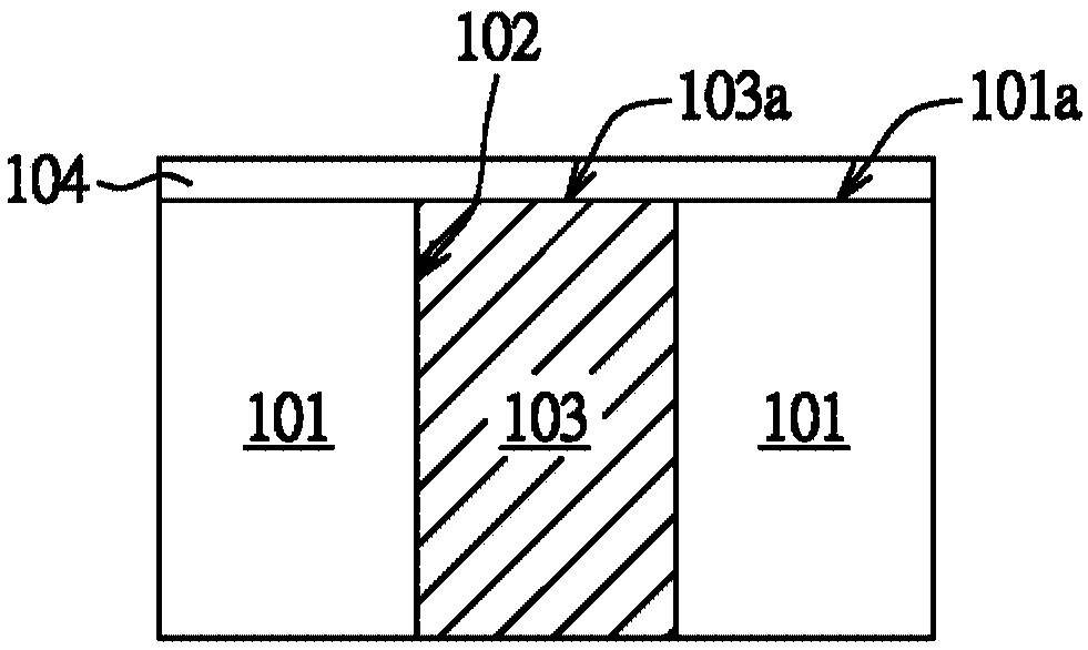
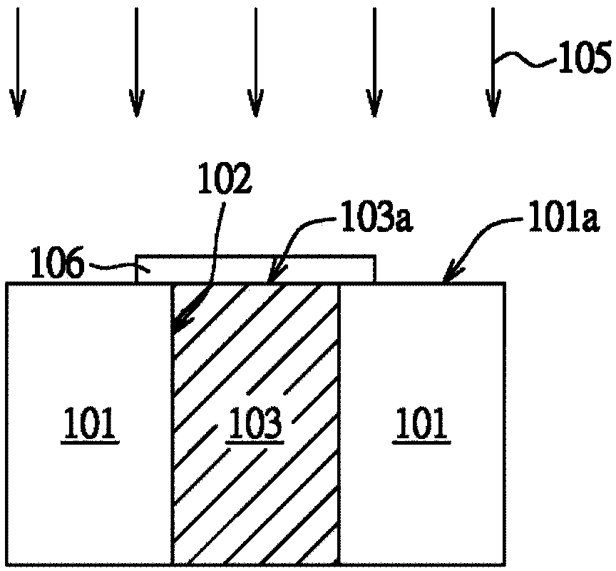
[0040] This description provides a resistive memory element and its manufacturing method, which can reduce the formation voltage of the memory element and increase the bit density of the resistive memory element. In order to make the above-mentioned embodiment and other objects, features and advantages of this specification more comprehensible, a memory device and its manufacturing method are specifically cited as a preferred embodiment below, and are described in detail with the accompanying drawings.

[0041] However, it must be noted that these specific implementation cases and methods are not intended to limit the present invention. The invention can still be implemented with other features, elements, methods and parameters. The proposal of the preferred embodiment is only used to illustrate the technical characteristics of the present invention, and is not intended to limit the patent scope of the present invention. Those skilled in the art will be able to make equivalen...


PUM

PropertyMeasurementUnit
thicknessaaaaaaaaaa
thicknessaaaaaaaaaa
thicknessaaaaaaaaaa

Abstract

A resistive memory includes a first electrode layer, a first transition metal oxide layer, a second transition metal oxide layer, and a second electrode layer, wherein the first electrode layer comprises tungsten (Tungsten, W); the first transition metal oxide (TMO) layer is located on the first electrode layer and comprises titanium (Titanium, Ti); the second transition metal oxide layer is located on the first transition metal oxide layer and comprises silicon (Silicon, Si); the second electrode layer is on the second transition metal oxide layer and does not include tungsten; and the firsttransition metal oxide layer has a greater dielectric constant than the second transition metal oxide layer.

Description

technical field [0001] The disclosure relates to a non-volatile memory (non-volatile memory, NVM) and a manufacturing method thereof. In particular, it relates to a resistive memory element (resistive memory) and a manufacturing method thereof. Background technique [0002] A non-volatile memory device has the characteristic that the information stored in the memory unit will not be lost when the power is removed. At present, the charge trap flash (CTF) memory device that uses a charge trap is more widely used. However, as the accumulation density of the memory device increases, the critical size and pitch of the device shrink, and the charge storage flash memory device faces its physical limit and cannot operate. [0003] Resistive memory elements, such as resistive random-access memory (ReRAM), apply a pulse voltage to the metal oxide film of the memory element to generate a resistance difference as an information storage state such as "0". and the interpretation basis ...

Claims


Application Information

Patent Timeline
Patent Type & Authority Applications(China)
IPC IPC(8): H01L45/00
CPCH10N70/8836H10N70/011H10N70/8833
Inventor 曾柏皓李峰旻
Owner MACRONIX INT CO LTD
Why Eureka
Try Eureka