Micro LED huge transfer device and method based on addressable electromagnetic array

A transfer device and array technology, applied in the field of mass transfer, can solve the problems of inaccuracy, increase the difficulty of manufacturing micro light-emitting diodes and molds, easy to miss positioning, etc. Effect

Active Publication Date: 2019-10-18
HUAZHONG UNIV OF SCI & TECH
View PDF7 Cites 11 Cited by
  • Summary
  • Abstract
  • Description
  • Claims
  • Application Information

AI Technical Summary

Problems solved by technology

[0004] At present, the mass transfer technology that can realize selective transfer mainly includes the following types: One is to realize selective transfer by making molds. This method positions micro LEDs by making left and right asymmetrical micro holes on the mold. The place where the LED is received on the circuit substrate, and vice versa, it is not received. This method requires the shape of the micro-LED to be consistent with the shape of the hole, which increases the difficulty of making the micro-LED and the mold; the second is to realize the selection through fluid self-assembly Sexual transfer, this method puts the micro-LEDs with magnetic poles and the circuit substrate into a specific solution, and is positioned by magnetic force, and the micro-light-emitting diodes positioned by the magnetic force are received, otherwise they are not received. and inaccurate positioning

Method used


Image

  • Micro LED huge transfer device and method based on addressable electromagnetic array
  • Micro LED huge transfer device and method based on addressable electromagnetic array
  • Micro LED huge transfer device and method based on addressable electromagnetic array

Examples


Embodiment Construction

[0040] In order to make the object, technical solution and advantages of the present invention clearer, the present invention will be further described in detail below in conjunction with the accompanying drawings and embodiments. It should be understood that the specific embodiments described here are only used to explain the present invention, not to limit the present invention. In addition, the technical features involved in the various embodiments of the present invention described below can be combined with each other as long as they do not constitute a conflict with each other.

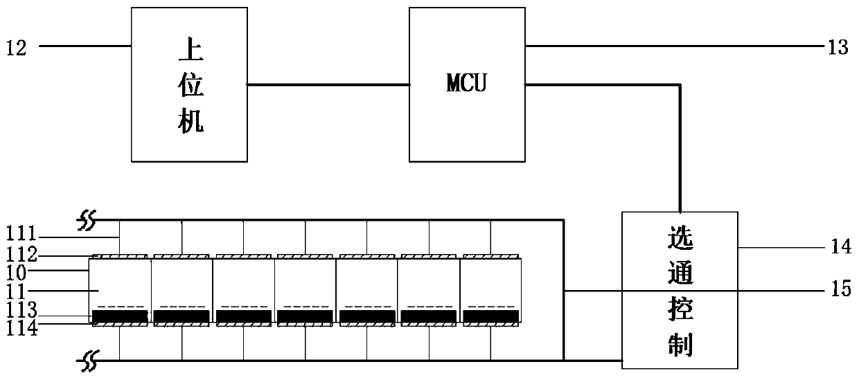
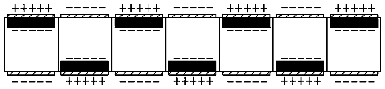
[0041] Such as figure 1 As shown, the embodiment of the present invention provides a MicroLED (miniature light-emitting diode) mass transfer device 10 based on an addressable electromagnetic array, wherein addressable means that individual control of each driving module (that is, independent control ). The device includes a host computer 12, a driver module array and a circuit module, wherein ...


PUM


Abstract

The invention belongs to the technical field of huge transfer, and particularly discloses a Micro LED huge transfer device and method based on an addressable electromagnetic array; the huge transfer device comprises an upper computer, a driving module array and a circuit module, wherein the driving module array is composed of a plurality of driving modules which are distributed in an array mode; an upper electrode and a lower electrode are arranged on each driving module, and an electrified electromagnet is arranged between the upper electrode and the lower electrode; the circuit module is connected with the upper computer and the driving modules separately, and is used for realizing independent control on the electric property of the electric charges of the upper electrode and the lower electrode of each driving module according to the control instruction of the upper computer, so that the magnetic force between the electrified electromagnet and the magnetic Micro LED can be changed,and the Micro LED can be picked and released. The method comprises the following steps of transferring the Micro LED to an intermediate carrier substrate; and transferring the Micro LED to a target circuit substrate by means of the device. The method disclosed by the invention can realize the patterning of the Micro LED and the selective huge transfer, and has the advantages of being convenient tooperate, high in applicability and the like.

Description

technical field [0001] The invention belongs to the technical field of mass transfer, and more specifically relates to a Micro LED mass transfer device and method based on an addressable electromagnetic array. Background technique [0002] In recent years, the manufacturing process of Micro LEDs (μLEDs) has become more and more perfect. Compared with traditional display panels, Micro LEDs have smaller size, higher resolution, higher brightness, higher luminous efficiency, and lower power consumption. And many other advantages, so it is also considered to be the mainstream of the next generation display technology. [0003] Usually, the manufacturing process of light-emitting diodes is to firstly thin the diode (LED) structure into a thin film, miniaturize, and array it so that its size is only about 10-20 microns, then transfer the micro-light-emitting diodes to the display circuit substrate in batches, and finally carry out encapsulation. Among them, how to realize batch ...

Claims


Application Information

Patent Timeline
Patent Type & Authority Applications(China)
IPC IPC(8): H01L21/683H01L21/67H01L25/075H01L33/48H01F13/00
CPCH01F13/006H01L21/67271H01L21/6835H01L21/6836H01L25/0753H01L33/48H01L2221/68368H01L2221/68381H01L2933/0033
Inventor 黄永安杨彪卞敬尹周平
Owner HUAZHONG UNIV OF SCI & TECH
Why Eureka
Try Eureka