Saturable absorber based on planar optical waveguide and preparation method thereof
A saturable absorption, planar optical waveguide technology, used in lasers, laser parts, semiconductor lasers, etc., can solve the problems of increasing the effective length of light and saturable absorbers, reducing thermal effects, etc., to improve the anti-laser damage threshold. , enhance the modulation depth, avoid the effect of thermal effects
- Summary
- Abstract
- Description
- Claims
- Application Information
AI Technical Summary
Problems solved by technology
Method used
Image
Examples
Embodiment 1
[0028] This example illustrates how to prepare an ITO saturable absorber based on a planar optical waveguide and use it in a 1.5 micron band fiber pulse laser.
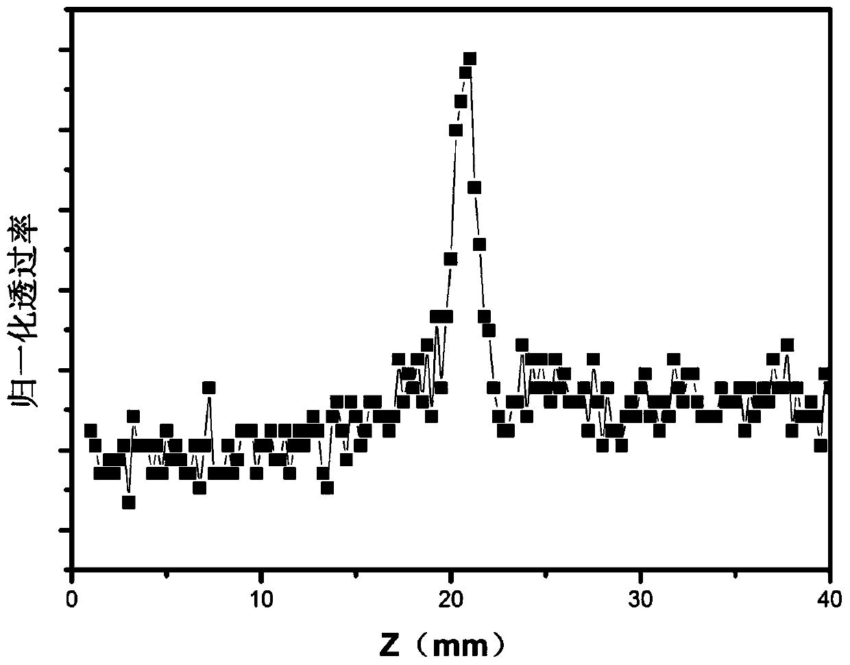
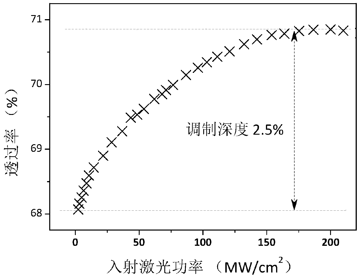
[0029] (1) Take 20 microliters of chemically synthesized ITO nanocrystalline toluene solution and drop it on a quartz plate to dry to form a film. Utilize femtosecond laser (220fs, 1300nm, 1kHz) to study the saturation absorption characteristics of ITO thin films by opening Z-scan technology, the results are as follows figure 1 As shown, obvious saturated absorption characteristics can be observed. Such as figure 2 As shown, by studying the relationship between the transmittance and the excitation power, it is confirmed again that the ITO thin film has excellent saturable absorption characteristics.
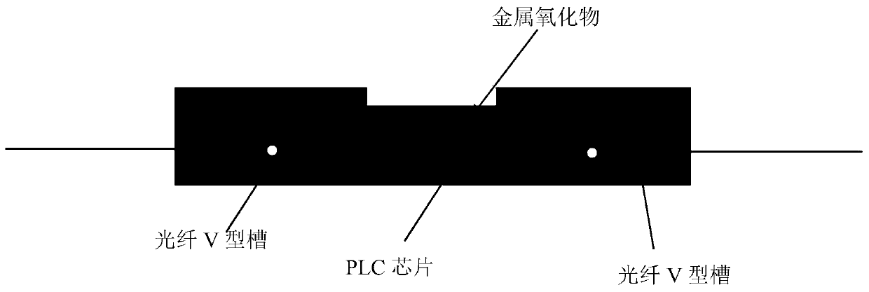
[0030] (2) if image 3 As shown, the waveguide is formed by etching the PLC chip by PECVD; take 20 microliters of chemically synthesized ITO nanocrystal toluene solution and drop it 10 microns above the waveguide for...
Embodiment 2
[0033] This example illustrates how to prepare an AZO saturable absorber based on a planar optical waveguide, and apply it to a solid-state laser with a wavelength of 1.0 micron to realize Q-switched pulse output.
[0034] (1) Take 20 microliters of chemically synthesized AZO nanocrystal toluene solution and drop it on the upper surface 10 microns away from the waveguide of the PLC chip. After drying, the AZO nanocrystal is covered on the upper surface of the waveguide as a saturable absorber device.
[0035] (2) The saturable absorber device obtained in (1) is integrated into a ring laser cavity to form a pulsed fiber laser (the gain fiber here is a Yb:YAP fiber), and a Q-modulated pulse is obtained under 980nm pumping Output, the laser wavelength is 1060nm, and the pulse width is 2.0 microseconds.
Embodiment 3
[0037] This example illustrates how to prepare an IZO saturable absorber based on a planar optical waveguide by using laser pulse deposition technology, and the working band covers 1.5-3.0 microns.
[0038] (1) Take a PLC chip with a thickness of 2 mm, a length of 10 mm, and a width of 5 mm, wherein the waveguide is formed by etching the PLC chip by PECVD.
[0039] (2) Deposit a layer of IZO nanocrystals at 10 microns above the waveguide of the PLC chip obtained in (1) by laser pulse deposition technology.
[0040] (3) Through the waveguide coupling platform, the PLC chip deposited with IZO nanocrystals and the optical fiber V-groove are coupled together to make an IZO saturable absorber with a planar optical waveguide.
[0041] (4) Based on the Tm-doped fiber, the planar optical waveguide IZO saturable absorber prepared in (2) was integrated into the ring fiber laser cavity, and the Q-switched pulse output in the 2.0 micron band was obtained with a pulse width of 4.0 microsec...
PUM
 Abstract
Description
Claims
Application Information
 - R&D
- Intellectual Property
- Life Sciences
- Materials
- Tech Scout
- Unparalleled Data Quality
- Higher Quality Content
- 60% Fewer Hallucinations
Browse by: Latest US Patents, China's latest patents, Technical Efficacy Thesaurus, Application Domain, Technology Topic, Popular Technical Reports.
© 2025 PatSnap. All rights reserved.Legal|Privacy policy|Modern Slavery Act Transparency Statement|Sitemap|About US| Contact US: help@patsnap.com


