Silicon wafer processing device and method

A technology for processing devices and silicon wafers, which is applied in the direction of transportation and packaging, conveyor objects, electrical components, etc., can solve the problems of silicon wafer edge warping and edge collapse, so as to improve flatness and prevent edge warping or edge collapse , the effect of precision processing

Inactive Publication Date: 2019-10-22
XIAN ESWIN MATERIAL TECH CO LTD +1
View PDF4 Cites 1 Cited by
  • Summary
  • Abstract
  • Description
  • Claims
  • Application Information

AI Technical Summary

Problems solved by technology

[0003] Embodiments of the present invention provide a silicon wafer processing device and method to solve the problems of edge warping and edge collapse during the grinding process of silicon wafers

Method used


Image

  • Silicon wafer processing device and method
  • Silicon wafer processing device and method
  • Silicon wafer processing device and method

Examples


Embodiment Construction

[0042] In order to make the technical problems, technical solutions and advantages to be solved by the present invention clearer, the following will describe in detail with reference to the drawings and specific embodiments.

[0043] The terms "first", "second" and the like in the description and claims of the present invention are used to distinguish similar objects, and are not necessarily used to describe a specific order or sequence. It is to be understood that the data so used are interchangeable under appropriate circumstances such that the embodiments of the invention described herein are, for example, capable of practice in sequences other than those illustrated or described herein.

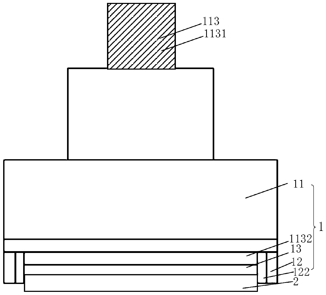
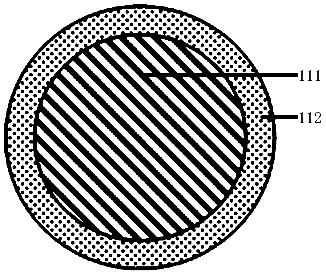
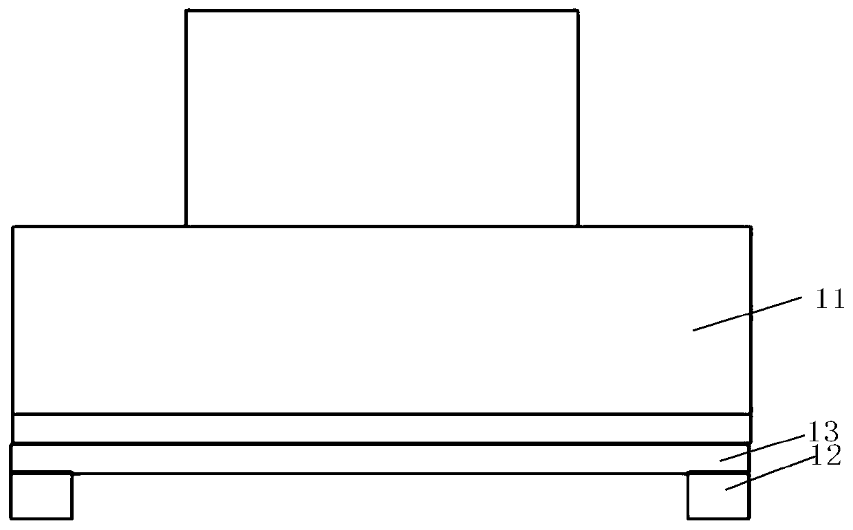
[0044] see figure 1 with figure 2 , the embodiment of the present invention provides a silicon wafer processing device 1 , the silicon wafer processing device 1 may be a final polishing machine, and the silicon wafer processing device 1 includes: a polishing head 11 , an annular mold 12...


PUM


Abstract

The embodiment of the invention provides a silicon wafer processing device and method. The silicon wafer processing device comprises an annular mold, a polishing head and a mold pad, wherein the polishing head includes a central control area and an edge area arranged around the central control area, and the edge area of the polishing head is attached and connected to the axial end face of the annular mold; the central control area of the polishing head is provided with an adjustment structure; the mold pad is located in the annular mold and is arranged in a mode of being independent from the annular mold, the first end face of the mold pad is attached and connected to the adjustment structure, the adjustment structure is used for driving the mold pad to move towards a first direction or asecond direction opposite to the first direction along the axial direction of the polishing head to adjust the height difference between the annular mold and the mold pad, the second end face, which is opposite to the first end face, of the mold pad forms an accommodating space with the inner wall of the annular mold, a silicon wafer is arranged in the accommodating space, and the first end face of the silicon wafer is attached and connected to the second end face of the mold pad. Therefore, the phenomenon of edge tilting or edge collapse of the silicon wafer in the grinding process can be prevented, and the flatness of the silicon wafer is improved.

Description

technical field [0001] The invention relates to the field of final polishing equipment processing silicon wafers, in particular to a silicon wafer processing device and method. Background technique [0002] During the grinding process of silicon wafers (for example: in the final polishing process of silicon wafers), due to the unreasonable structure of the combined mold pad used to absorb and restrain the silicon wafers, the edge of the silicon wafers often rises and falls. . Contents of the invention [0003] Embodiments of the present invention provide a silicon wafer processing device and method to solve the problems of edge warping and edge collapse during the silicon wafer grinding process. [0004] In the first aspect, in order to solve the above technical problems, an embodiment of the present invention provides a silicon wafer processing device, including: [0005] ring mold; [0006] The polishing head includes: a central control area and an edge area arranged ...

Claims


Application Information

Patent Timeline
Patent Type & Authority Applications(China)
IPC IPC(8): H01L21/67H01L21/677H01L21/02
CPCH01L21/02H01L21/67H01L21/67011H01L21/67242H01L21/67253H01L21/677
Inventor 李昀泽
Owner XIAN ESWIN MATERIAL TECH CO LTD
Why Eureka
Try Eureka