Visual processing device, display device, and integrated circuit

a technology of display device and visual processing device, which is applied in the field of visual processing device, display device, integrated circuit, can solve problems such as discrepancy between, and achieve the effect of precise contrast adjustmen

Active Publication Date: 2007-04-12
PANASONIC INTELLECTUAL PROPERTY CORP OF AMERICA
View PDF6 Cites 69 Cited by
  • Summary
  • Abstract
  • Description
  • Claims
  • Application Information

AI Technical Summary

Benefits of technology

[0012] With this visual processing device, a first gain signal having predetermined gain characteristics for the image signal is output, and the image signal that has been input to the visual processing device is corrected based on the first gain signal, and thus it is possible to achieve precise correction processing with a simple structure. That is, image signals are corrected using a gain signal rather than through direct correction of the grayscale, and this allows image signals to be corrected through simple processing and allows the scale of the circuit to be reduced if hardware is used, for example. Since the correction of image signals is achieved through correction by the gain signal, the output timing of the output image signals after correction can be synchronized with ease.
[0095] According to the invention, it is possible to achieve a visual processing device that can execute precise contrast adjustment on image signals that are input and that does not lead to discrepancies in the output timing of the image signals that are output. It is also possible to achieve a display device that is provided with this visual processing device, and an integrated circuit that includes this visual processing device.

Problems solved by technology

However, contrast adjustment circuits having the above configuration have the problem that for the color signal, the process of obtaining a coefficient for multiplication by the multiplier and then multiplying the color signal by the coefficient that has been obtained is performed after the luminance signal has been divided by the division circuit (the process of dividing the luminance signal includes numerous computations and as such it takes time before the result of the division is output, thus causing a delay), and therefore a discrepancy occurs between the output timing of the luminance signal to be output and the output timing of the color signals to be output, and, additionally, a delay means or the like for synchronizing the timing of the output luminance signal and the output color signals is necessary.

Method used


Image

  • Visual processing device, display device, and integrated circuit
  • Visual processing device, display device, and integrated circuit
  • Visual processing device, display device, and integrated circuit

Examples


first embodiment

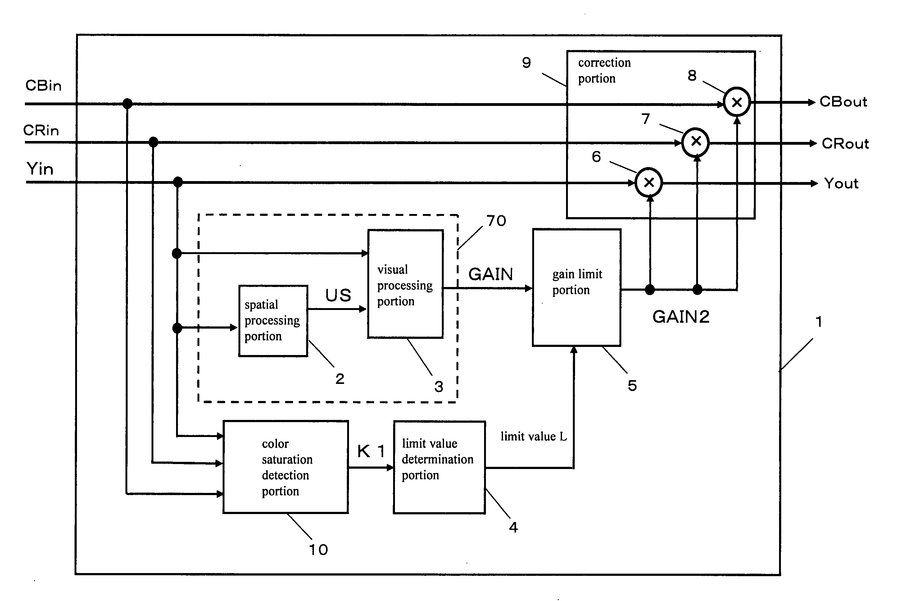
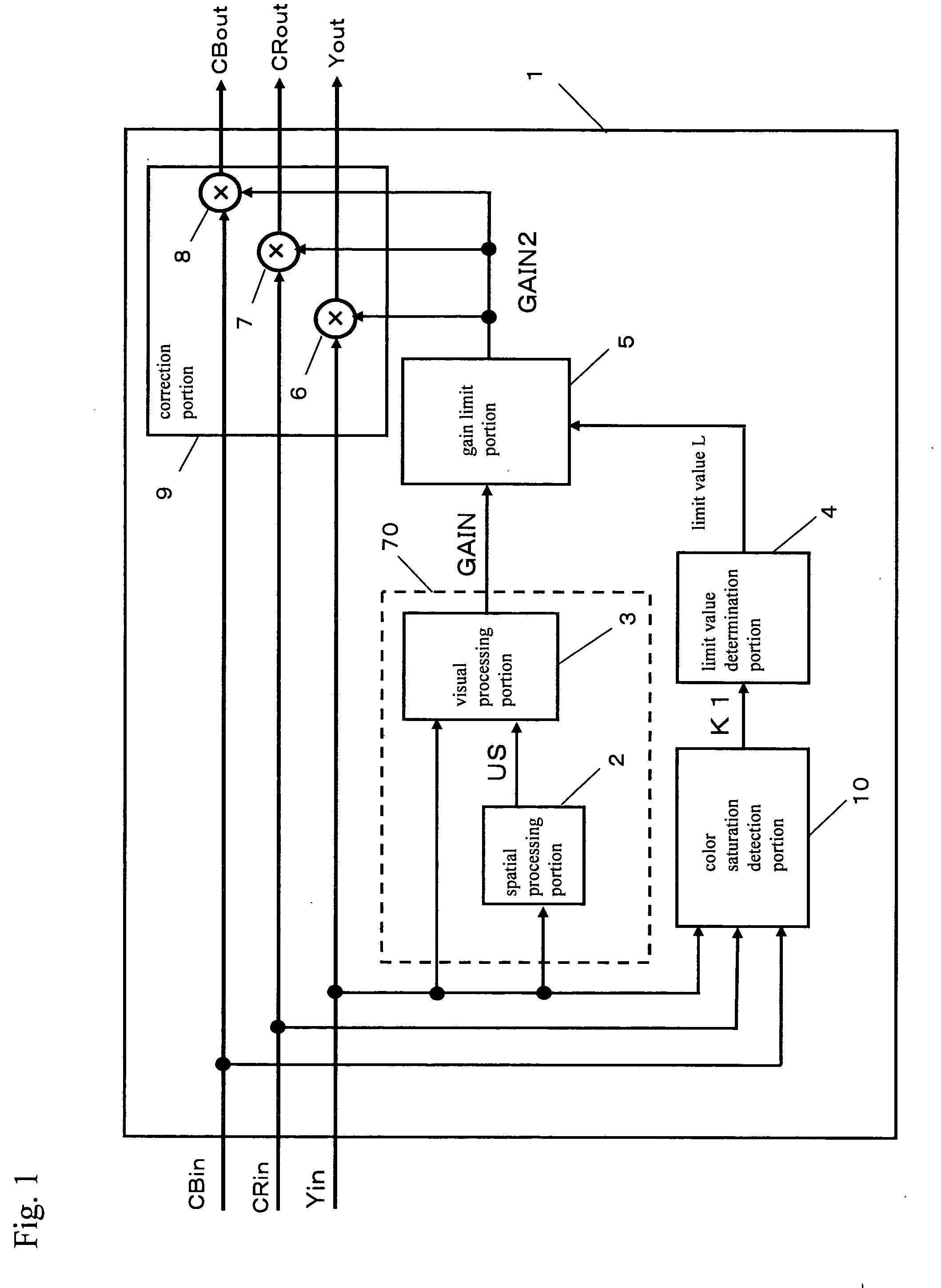
[0150] First, the visual processing device according to a first embodiment is described. The visual processing performed here is processing for giving characteristics that are close to human vision, and is for determining the value of an output signal according to the contrast between the value of a target pixel of an image signal that has been input and the values of pixels around that target pixel.

[0151] Examples of processing that may be adopted include backlight correction, knee processing, D range compression, color processing, and brightness adjustment (including gradation processing and contrast adjustment). It should be noted that in this invention, the luminance signal is defined as the Y component (the luminance component and the brightness component) in a YCbCr color space, a YUV color space, a Lab color space, a Luv color space, a YIQ color space, and a YPbPr color space.

[0152] Similarly, the color signal is defined as the CbCr component in a YCbCr color space, the UV ...

second embodiment

[0228] A display device according to a second embodiment of the invention is described next using FIGS. 13 to 17. Components that are the same as in the first embodiment have been assigned the same reference numerals and are not described in detail.

[0229] In this second embodiment of the invention, an example of determining the limit value of the first gain signal GAIN of the visual processing device 1 is described using FIG. 13. FIG. 13 is a block diagram showing the configuration of a display device 30 according to a second embodiment of the invention.

[0230] In FIG. 13, the display device 30 is provided with a tuner 31 for receiving program information, a program information separating portion 32 for separating the program information, an AV decoding portion 33 for decoding video data and audio data, the visual processing device 1 for visually processing the video data, and an output portion 35 for displaying the processed image.

[0231] The display device 30 can also be furnishe...

third embodiment

[0265] As a third embodiment of the invention, a method of suppressing a drop in the contrast of the output signal Yout in a case where the spatial frequency band of the gain signal GAIN that is output from the gain-type visual processing portion 70 is limited and the value (signal level) of the luminance signal Yin that has been input is changed by a value (signal level) that is significantly larger than the value (signal level) of the unsharp signal US is described using FIGS. 18 to 20.

[0266]FIG. 18 is a block diagram showing the configuration of a gain-type visual processing portion 71, FIG. 19A is an explanatory diagram describing the range over which the gain-type visual processing portion 71 extracts the brightness information around the pixel in question, FIG. 19B is a diagram showing an example of the signal waveform of the Yin signal, the US signal, and the USH signal in the gain-type visual processing portion 71, FIG. 20A is an explanatory diagram describing the grayscale...


PUM


Abstract

The invention achieves a visual processing device that can execute precise contrast adjustment on image signals that have been input and that does not cause discrepancies in the output timing of the image signals that are output. The visual processing device is provided with a gain-type visual processing portion that outputs a first gain signal having predetermined gain characteristics with respect to the input image signal, and a correction portion that corrects the input image signal based on the first gain signal.

Description

BACKGROUND OF THE INVENTION [0001] 1. Field of the Invention [0002] The present invention relates to visual processing devices, display devices, and integrated circuits, and in particular relates to visual processing devices, display devices, and integrated circuits in which the contrast of an image is adjusted. [0003] 2. Description of the Related Art [0004] Conventional color television receivers have performed contrast adjustment in order to adjust the image contrast. [0005] With contrast adjustment, RGB signals are separated into a luminance signal and color signals without disrupting the color balance, and then the contrast of the luminance signal is adjusted. [0006] Color appears light in areas where the luminance signal level has been increased and, conversely, appears dark in areas where the luminance signal level has been reduced, and leads to an output that is unnatural, and thus the level of the color signal also is increased or decreased in correspondence with the change...

Claims


Application Information

Patent Timeline
Patent Type & Authority Applications(United States)
IPC IPC(8): G06K9/40G09G5/02G06T5/00H04N5/20G09G3/20G09G5/00G09G5/36H04N5/243H04N5/57H04N9/04H04N9/68H04N9/77
CPCG09G5/04G09G5/06G09G2320/0242G09G2320/0285G09G2320/066G09G2320/0673H04N5/4401H04N5/57H04N9/643H04N9/68H04N9/69H04N21/4318H04N21/44008H04N21/84H04N21/426
Inventor YAMASHITA, HARUOITO, TAKESHIMONOBE, YUSUKEWATANABE, TATSUMIKUWAHARA, YASUHIRO
Owner PANASONIC INTELLECTUAL PROPERTY CORP OF AMERICA
Why Eureka
Try Eureka