Nitride thin-film solar cell
A solar cell and nitride technology, applied in the field of optical materials, can solve problems such as lattice mismatch, and achieve the effect of simplifying the process
- Summary
- Abstract
- Description
- Claims
- Application Information
AI Technical Summary
Problems solved by technology
Method used
Image

Examples
Embodiment 1
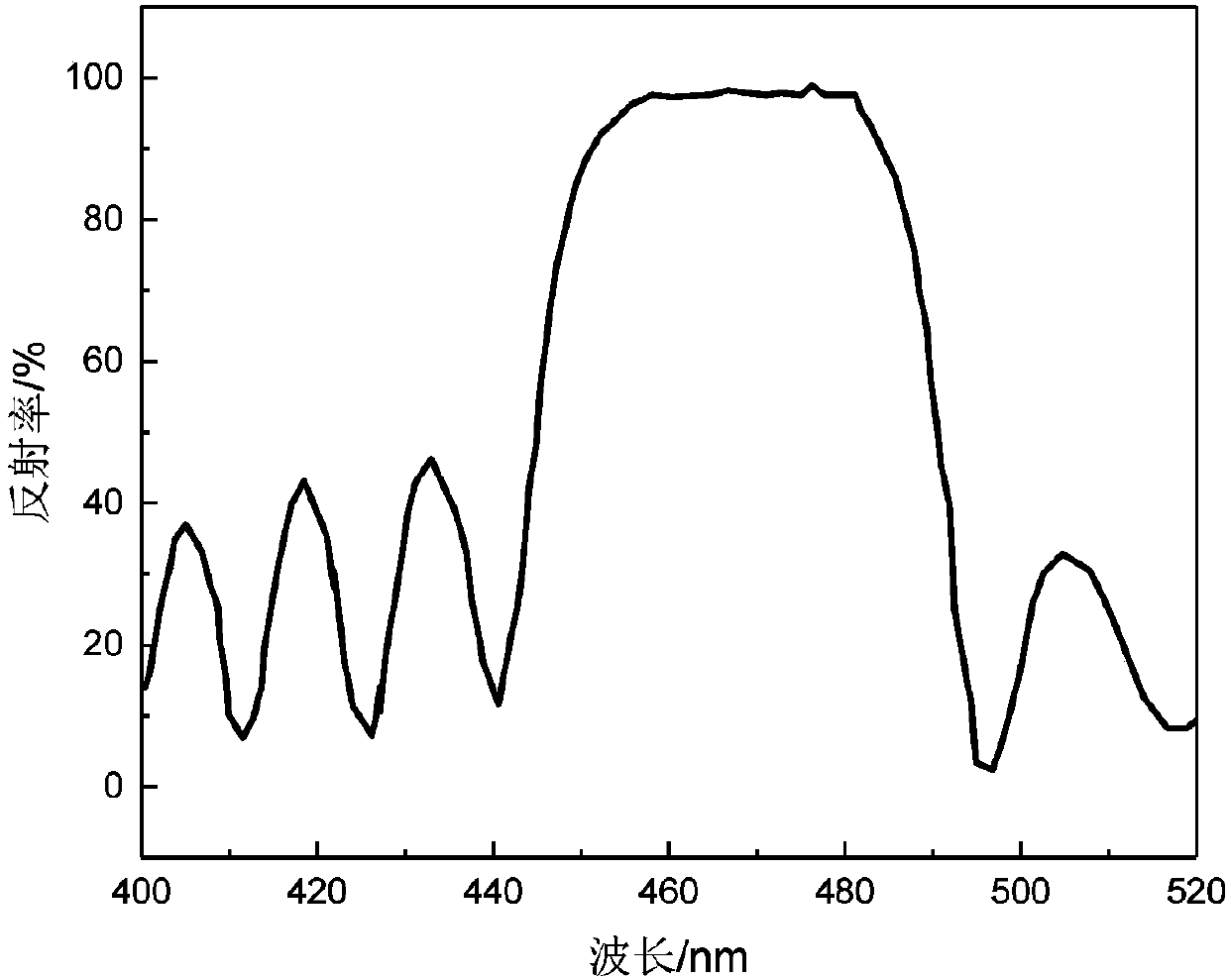
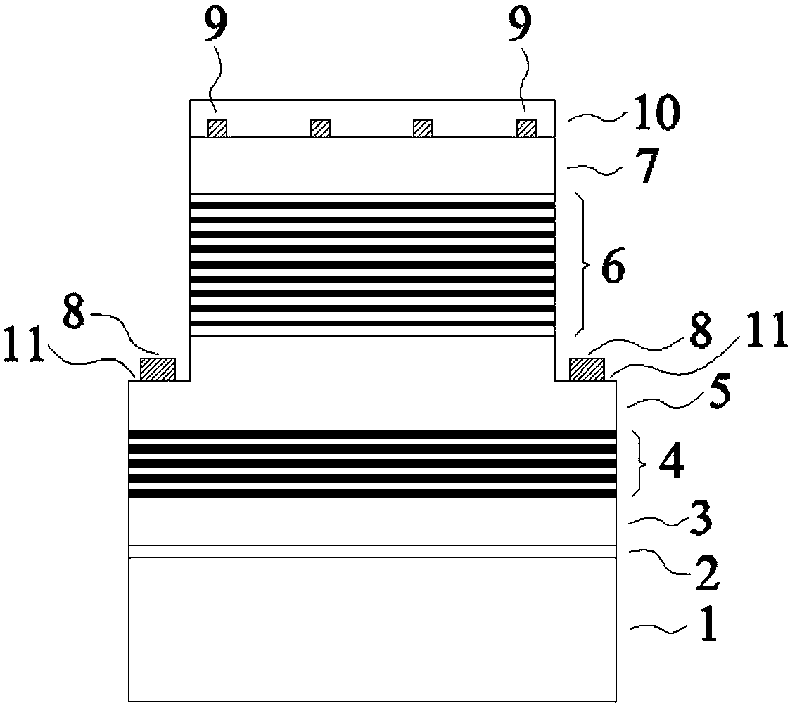
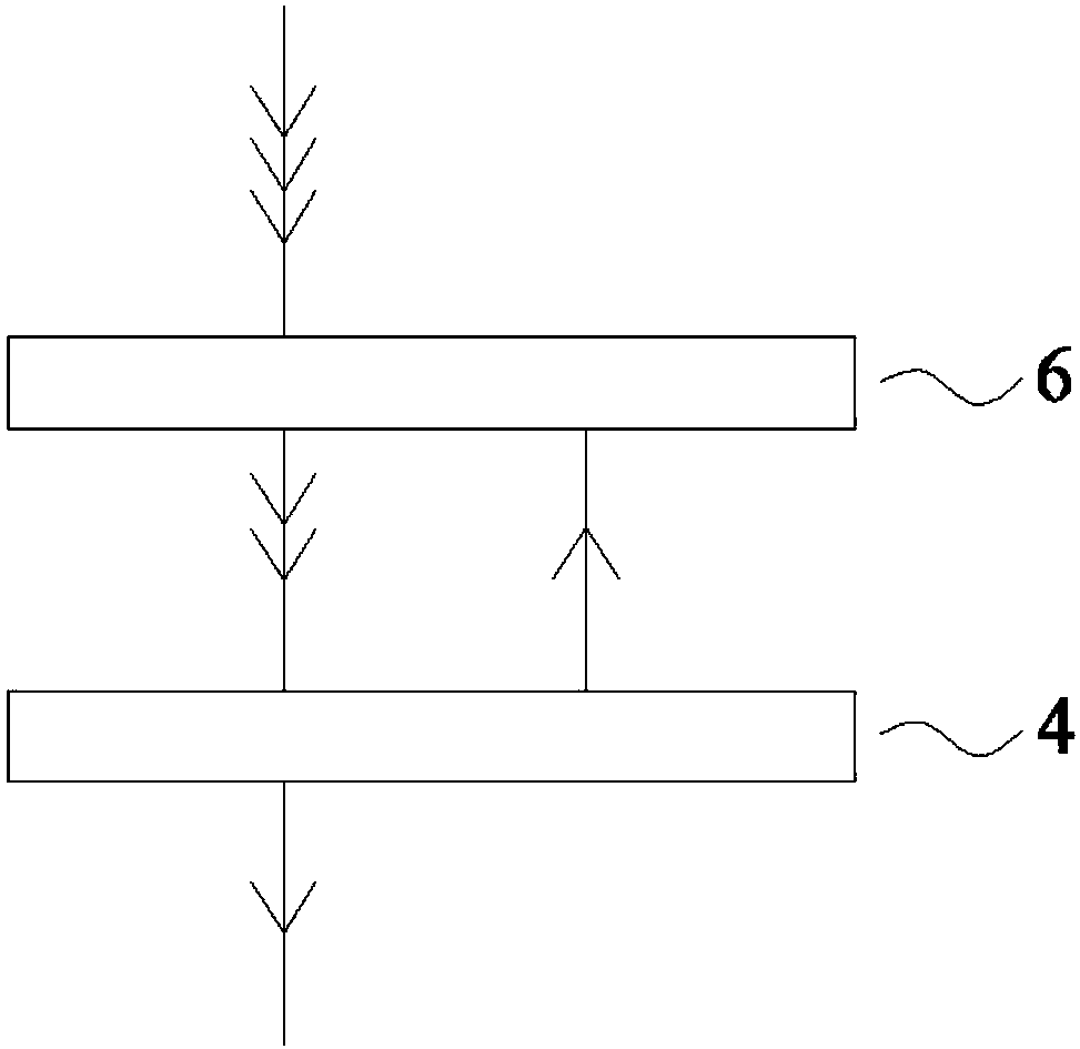
[0039] Such as figure 2 As shown, a specific embodiment of the present invention is a nitride thin film solar cell, comprising:
[0040] A substrate 1. The substrate 1 is a square sapphire substrate with a thickness of 600 μm and a side length of 100 mm. The front side of the substrate is in the direction of the c-plane (001). Before the growth of the epitaxial film, the sapphire substrate is subjected to grinding, polishing, and cleaning processes, and the surface condition meets the requirements for the growth of the nitride epitaxial layer. The non-doped layer, Bragg reflector (DBR), n-type doped layer, non-doped multiple quantum well layer and p-type doped layer are arranged in sequence from bottom to top on the substrate, and the above layers are deposited in the same vapor deposition equipment Ingrown.
[0041] The non-doped layer also includes a nucleation layer 2, the nucleation layer 2 is fabricated on the sapphire substrate, the non-doped layer 3 is fabricated on ...
Embodiment 2
[0052] structured as figure 2 As shown, another specific embodiment of the present invention is a nitride thin film solar cell, comprising:
[0053] A substrate 1, the substrate 1 is a square 4H-SiC substrate with a thickness of 600 μm and a side length of 100 mm, and the front side of the substrate is in the c-plane (001) direction. Before the growth of the epitaxial film, the 4H-SiC substrate was processed by grinding, polishing and cleaning, and the surface condition met the requirements for the growth of the nitride epitaxial layer.
[0054] A non-doped layer 3, the non-doped layer 3 adopts a high-temperature GaN layer with a thickness of 1.5 μm, the high-temperature GaN layer is prepared by metal-organic chemical vapor deposition (MOCVD) equipment, and the growth temperature of the high-temperature GaN layer is 1080 °C, the growth pressure is 200 Torr.
[0055] Preferably, the non-doped layer also includes a nucleation layer 2, the nucleation layer 2 adopts a low-tempe...
Embodiment 3
[0065] A nitride thin film solar cell, comprising:
[0066] A substrate 1. The substrate 1 is a square sapphire substrate with a thickness of 600 μm and a side length of 100 mm. The front side of the substrate is in the direction of the c-plane (001). The non-doped layer, Bragg reflector (DBR), n-type doped layer, non-doped multi-quantum well layer and p-type doped layer arranged sequentially from bottom to top on the substrate are grown in the same vapor deposition equipment.
[0067] The non-doped layer 3 also includes a nucleation layer 2, which is made on a sapphire substrate, and the nucleation layer 2 is a low-temperature Al with a thickness of 25 nm. 0.1 Ga 0.9 N layer, nucleation layer can also use Al 0.1 Ga 0.85 In 0.05 N, Ga 0.85 In 0.15 N and other film layers, nucleation layer 2 growth using metal organic chemical vapor deposition (MOCVD) equipment, low temperature Al 0.1 Ga 0.9 The growth temperature of the N layer is 500-7000°C, and the growth pressure is...
PUM
| Property | Measurement | Unit |
|---|---|---|
| Thickness | aaaaa | aaaaa |
| Thickness | aaaaa | aaaaa |
| Thickness | aaaaa | aaaaa |
Abstract
Description
Claims
Application Information
 - R&D Engineer
- R&D Manager
- IP Professional
- Industry Leading Data Capabilities
- Powerful AI technology
- Patent DNA Extraction
Browse by: Latest US Patents, China's latest patents, Technical Efficacy Thesaurus, Application Domain, Technology Topic.
© 2024 PatSnap. All rights reserved.Legal|Privacy policy|Modern Slavery Act Transparency Statement|Sitemap