Antistatic epitaxial structure and manufacturing method thereof

An epitaxial structure and manufacturing method technology, applied in circuits, electrical components, semiconductor devices, etc., can solve the problems of weak anti-static capability of epitaxial structures, quantum well burnout, chip failure, etc., to improve electrostatic capability and prevent electrostatic breakdown. , the effect of easy mass production

Pending Publication Date: 2019-10-22
FOSHAN NATIONSTAR SEMICON
View PDF0 Cites 2 Cited by
  • Summary
  • Abstract
  • Description
  • Claims
  • Application Information

AI Technical Summary

Problems solved by technology

[0003] Due to the weak antistatic ability of the epitaxial structure of the existing LED chips, the static electricity is injected from the U-shaped GaN layer, and other epitaxial structures cannot spread t

Method used


Image

  • Antistatic epitaxial structure and manufacturing method thereof
  • Antistatic epitaxial structure and manufacturing method thereof
  • Antistatic epitaxial structure and manufacturing method thereof

Examples


Embodiment 1

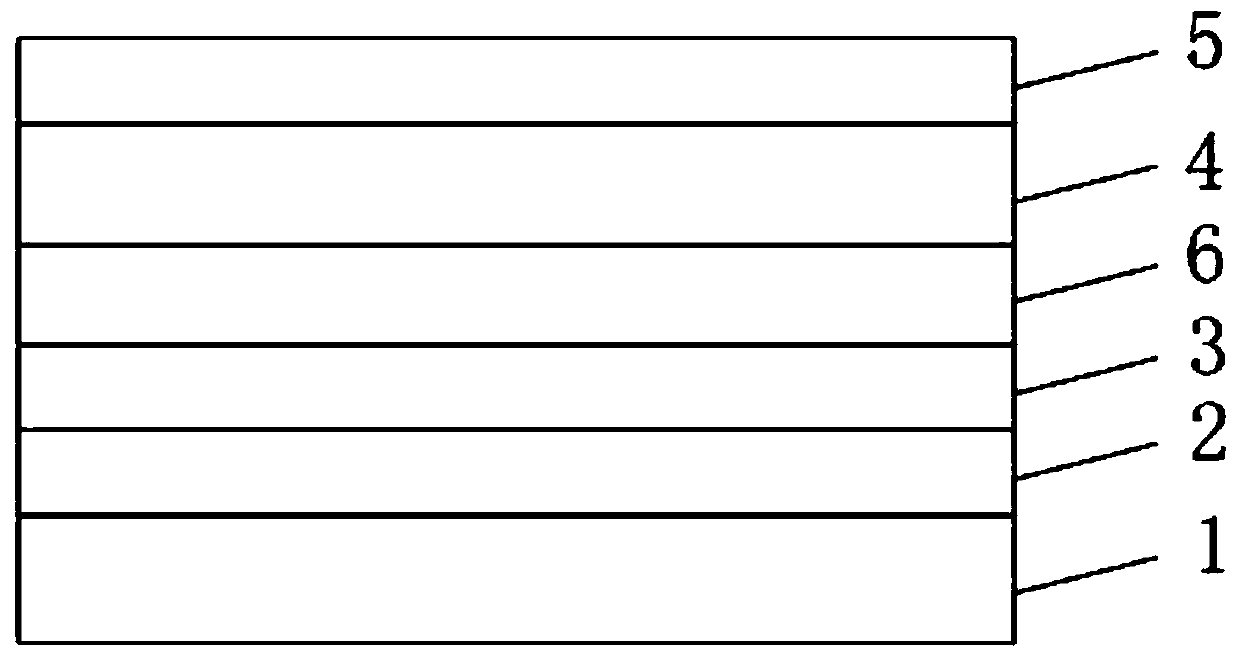
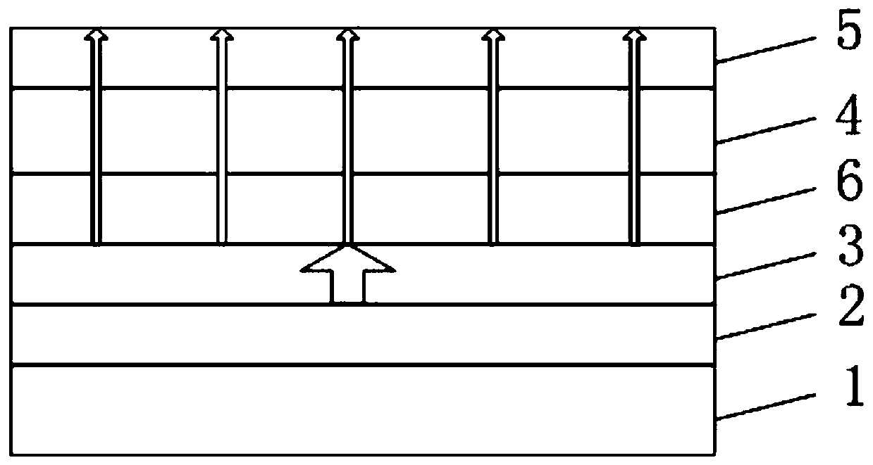
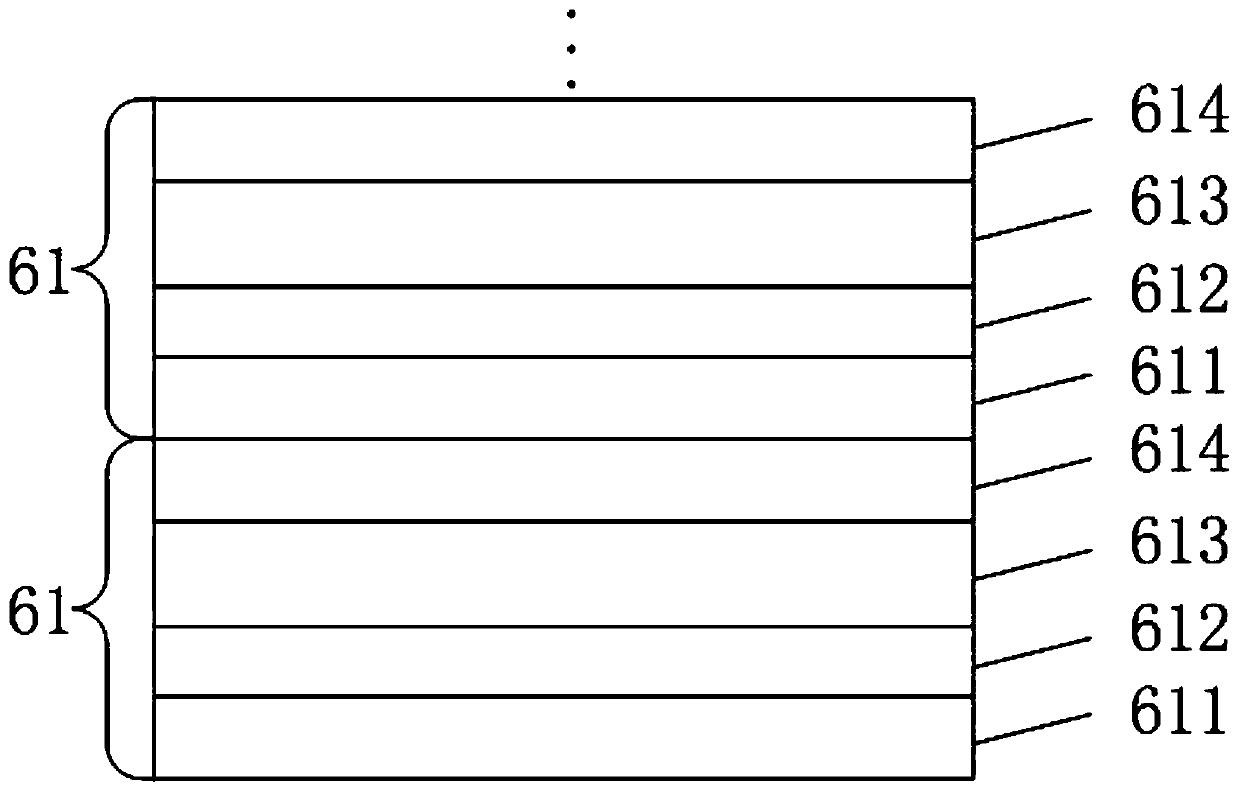
[0059] An antistatic epitaxial structure, comprising a buffer layer, an N-type GaN layer, an active layer and a P-type GaN layer sequentially arranged on a substrate, a composite layer is arranged between the N-type GaN layer and the active layer, The composite layer includes five GaN layers with varying silicon concentration, and the GaN layer with varying silicon concentration includes a first GaN layer, a second GaN layer disposed on the first GaN layer, and a third GaN layer disposed on the second GaN layer. layer, and a fourth GaN layer arranged on the third GaN layer, the doping concentration of silicon in the first GaN layer is 0, the doping concentration of silicon in the second GaN layer is 3E+15mor, the The doping concentration of silicon in the third GaN layer is 3E+19 mor, and the doping concentration of silicon in the fourth GaN layer is 3E+15 mor.

Embodiment 2

[0061] An antistatic epitaxial structure, comprising a buffer layer, a U-type GaN layer, an N-type GaN layer, an active layer and a P-type GaN layer sequentially arranged on a substrate, the U-type GaN layer and the N-type GaN layer A composite layer is provided between them, and the composite layer includes 5 layers of GaN layers with varying silicon concentrations, and the GaN layers with varying silicon concentrations include a first GaN layer, a second GaN layer disposed on the first GaN layer, and a GaN layer disposed on the second GaN layer. The third GaN layer on the layer, and the fourth GaN layer arranged on the third GaN layer, the doping concentration of silicon in the first GaN layer is 0, and the doping concentration of silicon in the second GaN layer is 3E+15 mor, the doping concentration of silicon in the third GaN layer is 3E+19 mor, and the doping concentration of silicon in the fourth GaN layer is 3E+15 mor.

Embodiment 3

[0063] An antistatic epitaxial structure, comprising a buffer layer, a U-type GaN layer, an N-type GaN layer, an active layer and a P-type GaN layer sequentially arranged on a substrate, between the N-type GaN layer and the active layer A composite layer is provided, and a composite layer is provided between the U-type GaN layer and the N-type GaN layer, and the composite layer includes 5 layers of GaN layers with silicon concentration changes, and the GaN layers with silicon concentration changes include the first GaN layer, the A second GaN layer on the first GaN layer, a third GaN layer on the second GaN layer, and a fourth GaN layer on the third GaN layer, the doping of silicon in the first GaN layer concentration is 0, the doping concentration of silicon in the second GaN layer is 3E+15mor, the doping concentration of silicon in the third GaN layer is 3E+19mor, and the doping concentration of silicon in the fourth GaN layer is equal to It is 3E+15mor.


PUM

PropertyMeasurementUnit
Thicknessaaaaaaaaaa
Thicknessaaaaaaaaaa
Thicknessaaaaaaaaaa

Abstract

The invention discloses an antistatic epitaxial structure and a manufacturing method thereof. The epitaxial structure comprises a buffer layer, an N-type GaN layer, an active layer and a P-type GaN layer which are sequentially arranged on a substrate, characterized in that it is characterized in that it comprises, a composite layer is arranged between the N-type GaN layer and the active layer; thecomposite layer comprises a plurality of silicon concentration changing GaN layers. The silicon concentration change GaN layer comprises a first GaN layer, a second GaN layer arranged on the first GaN layer, a third GaN layer arranged on the second GaN layer, and a fourth GaN layer arranged on the third GaN layer. Wherein the doping concentration of silicon in the first GaN layer is zero, and thedoping concentration of silicon in the second GaN layer and the fourth GaN layer is smaller than the doping concentration of silicon in the third GaN layer. According to the invention, the compositelayer is arranged between the N-type GaN layer and the active layer, and the current can be uniformly distributed to the whole epitaxial structure after passing through the composite layer, so that the current cannot be concentrated on a certain region or point, the antistatic capability of the epitaxial structure is improved, and the active layer is prevented from being broken down by static electricity.

Description

technical field [0001] The invention relates to the technical field of light emitting diodes, in particular to an antistatic epitaxial structure and a manufacturing method thereof. Background technique [0002] LED (Light Emitting Diode, Light Emitting Diode) is a semiconductor device that uses carrier recombination to release energy to form light. LED chips have low power consumption, pure chromaticity, long life, small size, fast response time, energy saving and environmental protection, etc. Many advantages. [0003] Due to the weak antistatic ability of the epitaxial structure of the existing LED chip, the static electricity is injected from the U-shaped GaN layer, and other epitaxial structures cannot spread the current quickly and effectively, so that the current is concentrated in a small area or a point, resulting in this If the area current is too large, the quantum well will be burned out and the chip will fail. How to improve the antistatic capability of the epi...

Claims


Application Information

Patent Timeline
IPC IPC(8): H01L33/14H01L33/32H01L33/00
CPCH01L33/0075H01L33/14H01L33/325
Inventor 崔永进庄家铭
Owner FOSHAN NATIONSTAR SEMICON
Why Eureka
Try Eureka