Light emitting diode, display substrate, transfer device and method thereof

A technology for light-emitting diodes and display substrates, which is used in the manufacture of semiconductor devices, electrical components, semiconductor/solid-state devices, etc. bit, the effect of improving the alignment accuracy

Active Publication Date: 2019-10-22
BOE TECH GRP CO LTD +1
View PDF4 Cites 3 Cited by
  • Summary
  • Abstract
  • Description
  • Claims
  • Application Information

AI Technical Summary

Problems solved by technology

[0006] The technical problem to be solved by the embodiments of the present invention is to provide a light-emitting diode, a display substrate, a transfer device and a

Method used


Image

  • Light emitting diode, display substrate, transfer device and method thereof
  • Light emitting diode, display substrate, transfer device and method thereof
  • Light emitting diode, display substrate, transfer device and method thereof

Examples


Embodiment Construction

[0053] The specific implementation manners of the present invention will be further described in detail below in conjunction with the accompanying drawings and examples. The following examples are used to illustrate the present invention, but are not intended to limit the scope of the present invention. It should be noted that, in the case of no conflict, the embodiments in the present application and the features in the embodiments can be combined arbitrarily with each other.

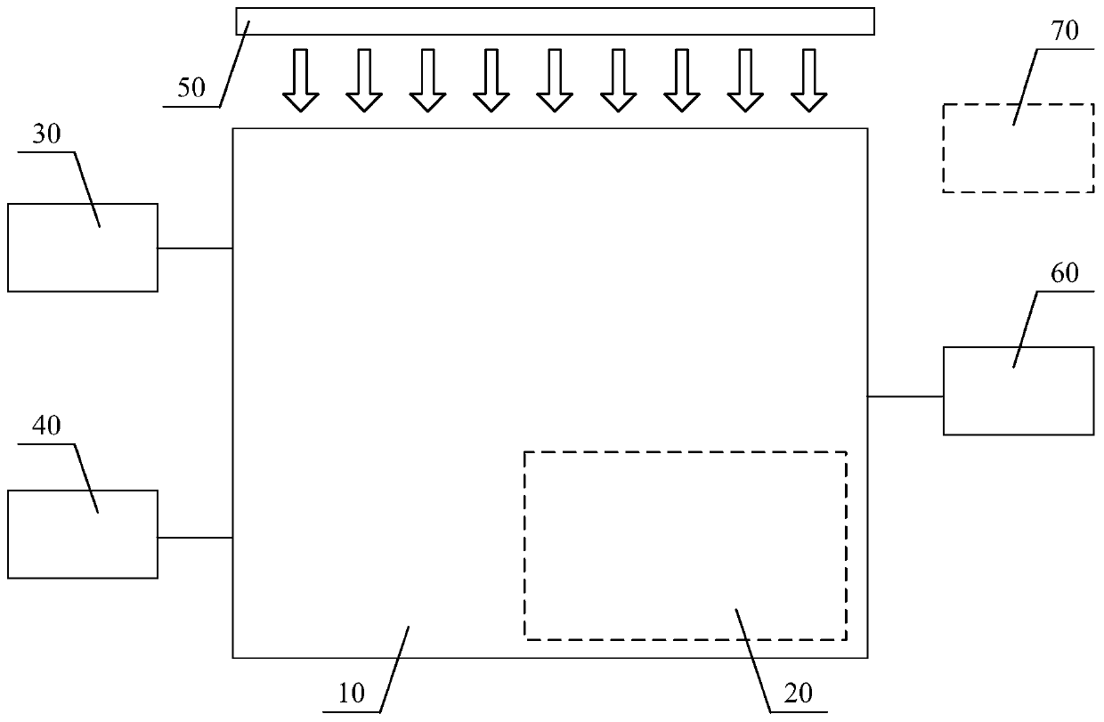
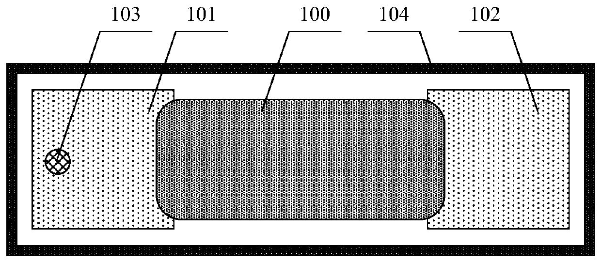
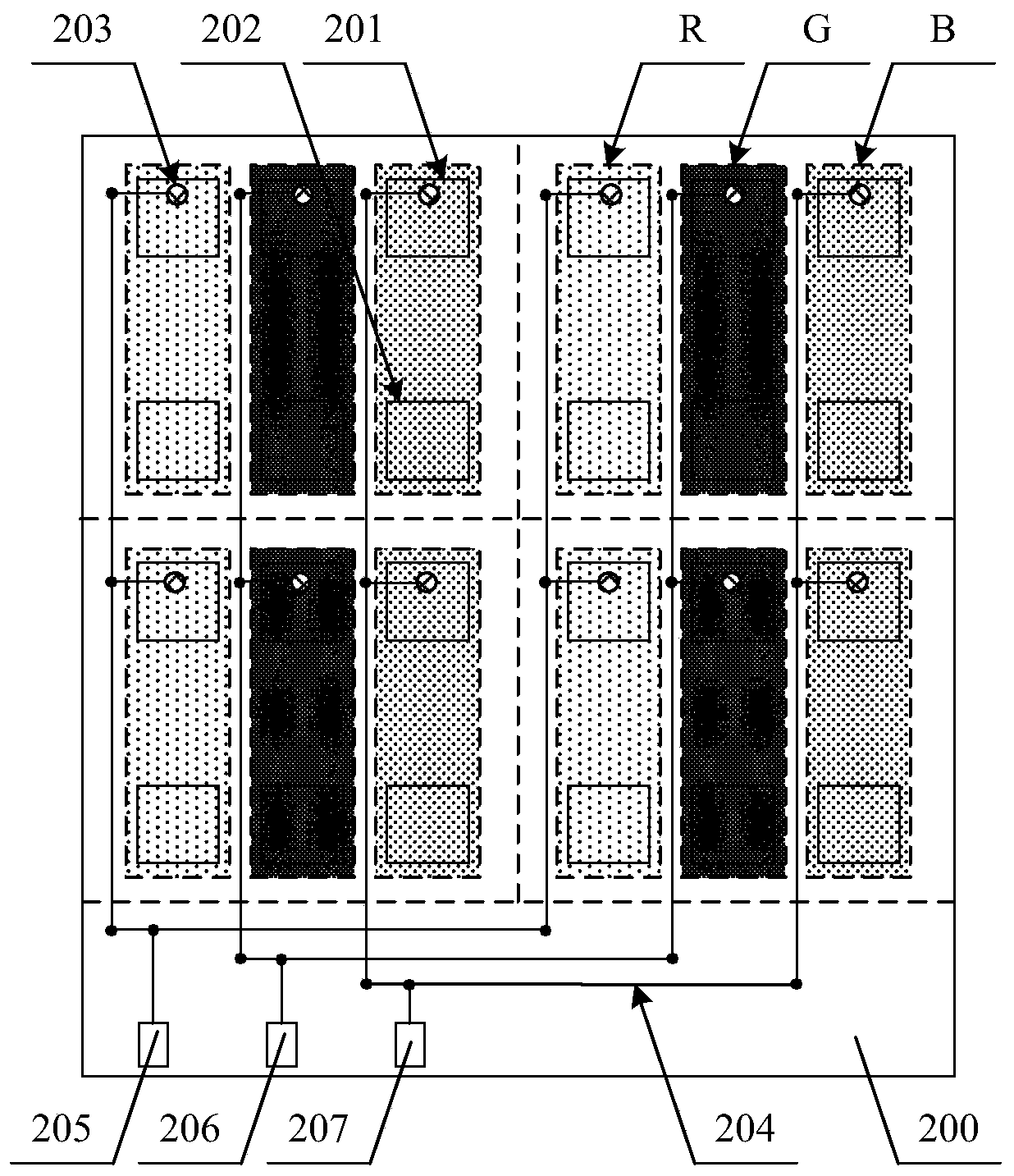
[0054] In order to overcome the problems of inaccurate alignment, low yield, long transfer time, high production cost, and unsuitability for large-scale mass production in the existing technical solutions, embodiments of the present invention provide a transfer device and method thereof. The transfer device in the embodiment of the present invention is used to transfer a plurality of light-emitting diodes to the display substrate, including an adsorption carrier, a sprinkler structure, a vibration mech...


PUM


Abstract

The embodiment of the invention provides a light emitting diode, a display substrate, a transfer device and a method thereof. The transfer device comprises an adsorption carrier plate for bearing andadsorbing a display substrate; a scattering structure which splashes a plurality of light emitting diodes to the display substrate; a vibration mechanism which drives the adsorption carrier plate to vibrate, so that the magnetic butt joint points of the light emitting diodes are adsorbed on electromagnetic blocks of the display substrate; and an alignment mechanism which drives the light emittingdiodes to deflect and be aligned by taking the magnetic abutting points as axes. According to the invention, the magnetic butt joint points are arranged on the light emitting diodes in advance; an electromagnetic block is arranged in each sub-pixel of the display substrate; the electromagnetic blocks in the sub-pixels adsorb the magnetic butt-joint points of the light-emitting diodes through the vibration of the adsorption carrier plate; the light emitting diodes are driven to deflect and be aligned by taking the magnetic butt joint points as the axes, so that accurate alignment of the light emitting diodes is realized, and the problems of inaccurate alignment, low yield, long transfer time, high production cost, unsuitability for large-scale mass production and the like in the prior art are effectively solved.

Description

technical field [0001] The invention relates to the field of display technology, in particular to a light emitting diode, a display substrate, a transfer device and a method thereof. Background technique [0002] Light Emitting Diode (LED) technology has been developed for nearly three decades, from the initial solid-state lighting power supply to the backlight source in the display field and then to the LED display screen, providing a solid foundation for its wider application. With the development of chip manufacturing and packaging technologies, sub-millimeter light emitting diode (Mini Light Emitting Diode, Mini LED) display and micro light emitting diode (Micro Light Emitting Diode, Micro LED) display have gradually become a hot spot of display panels. Among them, Micro LED display has significant advantages such as low power consumption, high color gamut, ultra-high resolution, and ultra-thin, and is expected to become a better display technology to replace Organic Lig...

Claims


Application Information

Patent Timeline
IPC IPC(8): H01L33/36H01L27/15H01L21/67
CPCH01L21/67144H01L27/156H01L33/36
Inventor 李蒙王晓霞于洁王遥遥李鹏涛秦树林黄庭峰
Owner BOE TECH GRP CO LTD
Why Eureka
Try Eureka