Wafer separation method
A separation method and wafer technology, which is applied in the manufacture of electrical components, electrical solid devices, semiconductor/solid devices, etc., can solve the problem of high cost of laser cutting, prevent the metal layer from lifting, reduce production costs, and ensure production quality Effect
- Summary
- Abstract
- Description
- Claims
- Application Information
AI Technical Summary
Problems solved by technology
Method used
Image

Examples
Embodiment Construction
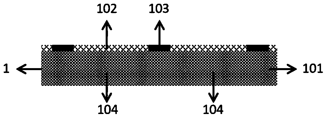
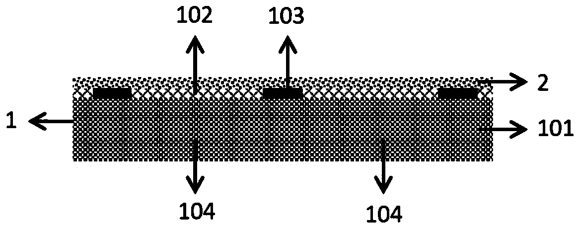
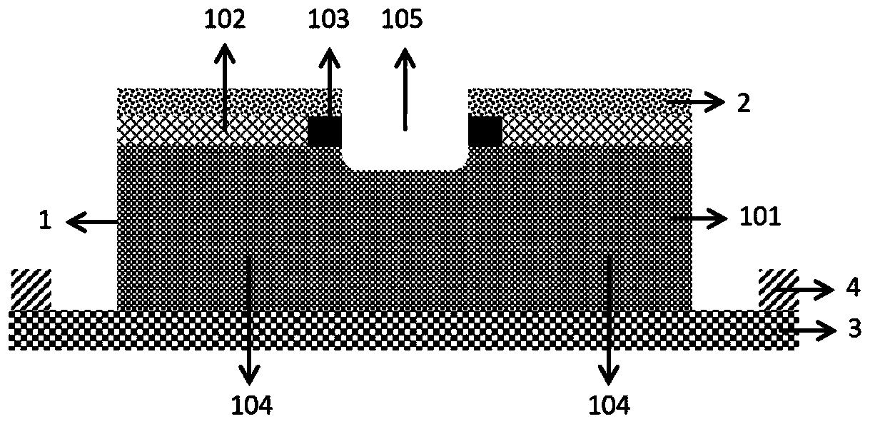
[0024] Such as figure 1 As shown, the wafer 1 targeted by the present invention is composed of a wafer substrate 101 and an upper circuit layer 102, and a series of dicing lines 103 are arranged in the circuit layer 102, and the dicing lines 103 include metal layers or / and low -k layers, these dicing streets 103 separate the entire wafer 1 into a plurality of chips 104 .
[0025] If the cutting line 103 is cut by mechanical cutting, due to the metal layer or / and low-k layer contained in the cutting line 103, problems such as lifting of the metal layer, chipping and / or peeling of the low-k layer, cracks, etc. will occur , affecting the performance and reliability of the chip, and greatly reducing the yield rate of the chip. Existing solutions are laser cutting or a combination of laser cutting and mechanical cutting, no matter which solution is inseparable from the use of laser cutting equipment, resulting in higher production costs.
[0026] In view of this problem, the solu...
PUM
| Property | Measurement | Unit |
|---|---|---|
| Thickness | aaaaa | aaaaa |
Abstract
Description
Claims
Application Information
 - R&D
- Intellectual Property
- Life Sciences
- Materials
- Tech Scout
- Unparalleled Data Quality
- Higher Quality Content
- 60% Fewer Hallucinations
Browse by: Latest US Patents, China's latest patents, Technical Efficacy Thesaurus, Application Domain, Technology Topic, Popular Technical Reports.
© 2025 PatSnap. All rights reserved.Legal|Privacy policy|Modern Slavery Act Transparency Statement|Sitemap|About US| Contact US: help@patsnap.com