Improved phosphor deposition system for leds

A phosphor layer and transparent conductor technology, which is applied in the field of color-changing light-emitting device packaging, can solve the problems of reducing the range of color adjustability between color endpoints, and achieve the effects of low cost, high mechanical robustness, and large thermal resistance

Active Publication Date: 2019-10-25
LUMILEDS
View PDF10 Cites 0 Cited by
  • Summary
  • Abstract
  • Description
  • Claims
  • Application Information

AI Technical Summary

Problems solved by technology

Additionally, optical crosstalk between the phosphors of adjacent LED pixels changes the color endpoints between packages and reduces the range of color tunability between color endpoints

Method used


Image

  • Improved phosphor deposition system for leds
  • Improved phosphor deposition system for leds
  • Improved phosphor deposition system for leds

Examples


Embodiment Construction

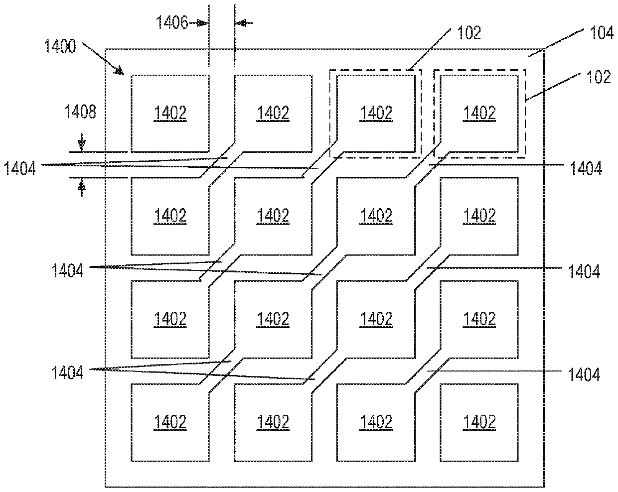
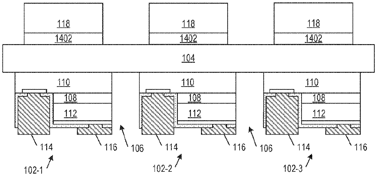
[0077] Picture 1-1 is a top view of a light emitting diode (LED) die 100 in some examples of the present disclosure. LED die 100 may be a segmented or multi-junction LED die. LED die 100 includes an array of junctions 102-1, 102-2, . ). The array of junctions 102 in LED die 100 is not limited to any size or shape. A trench 106 down to growth substrate 104 surrounds junction 102 such that they are fully electrically isolated from each other. Trenches 106 may be formed by wet etching, dry etching, mechanical sawing, laser scribing, or another suitable technique.

[0078] Figure 1-2 is a cross-sectional view of an LED die 100 in some examples of the present disclosure. Each junction 102 has a semiconductor structure including an active region 108 between an n-type semiconductor layer 110 and a p-type semiconductor layer 112 . Each junction 102 has a cathode 114 coupled to its n-type semiconductor layer 110 through an ohmic p-contact through an opening in the insulator (d...


PUM


Abstract

A method to produce a light-emitting device package includes mounting junctions on pads of a metalized substrate, where the junctions are at least partially electrically insulated from each other, andforming wavelength converters, where each wavelength converter is located over a different junction and separated by a gap from neighboring wavelength converters.

Description

technical field [0001] The present disclosure relates to color changing light emitting device packaging. Background technique [0002] Addressable color-changing LED structure [0003] There are several methods to construct color changing light emitting device packages. Many individual light-emitting diodes (LEDs) of different colors can be placed under a single primary optic. However, this has difficulty mixing colors. If there is no mixing, some primary optics will project different colors in different directions. When mixing is added, it makes the effective source size larger or compromises the design of the primary optics. The result is poor beam control or the need for larger primary optics. These affect the overall performance, form factor and price of the package. [0004] Alternatively, a number of individual LEDs of different colors may each be placed under its own primary optics. In this case, the beams may not completely overlap, especially at close distan...

Claims


Application Information

Patent Timeline
Patent Type & Authority Applications(China)
IPC IPC(8): H01L27/15H01L33/50
CPCH01L27/156H01L33/508H01L33/504H01L33/507H01L2224/95H01L2224/81H01L2224/16225H01L2224/1403H01L33/505H01L25/0753H01L33/58C25D13/22C25D13/12H01L33/62H01L2933/0058H01L2933/0066H01L2933/0041
Inventor K.J.瓦姆波拉N.佩西拉A.帕特尔
Owner LUMILEDS
Why Eureka
Try Eureka