Image segmentation method and device for background detection
A technology of image segmentation and background detection, which is applied in image analysis, image enhancement, image data processing, etc., can solve the problems of destroying area boundaries, difficult image segmentation, and large amount of calculation, so as to ensure image quality, facilitate detection, reduce The effect of the number of features
- Summary
- Abstract
- Description
- Claims
- Application Information
AI Technical Summary
Problems solved by technology
Method used
Image
Examples
no. 1 example
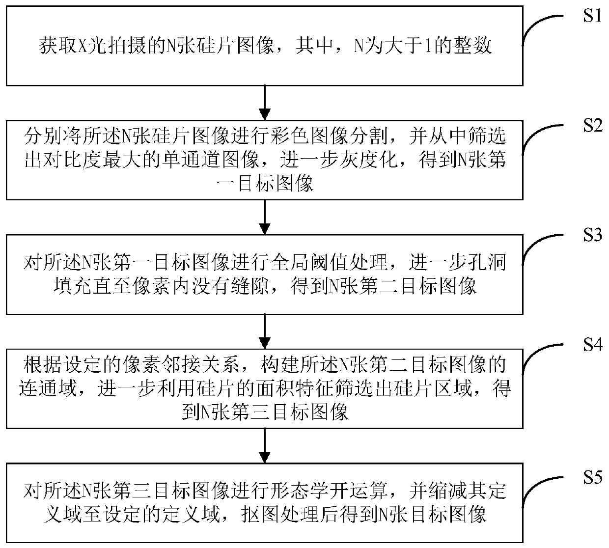
[0021] For a first example, see figure 1 .
[0022] Such as figure 1 As shown, the image segmentation method based on background detection provided by the first embodiment includes the following steps S1-S5:
[0023] S1. Acquire N silicon wafer images taken by X-rays, where N is an integer greater than 1.
[0024] S2. Carry out color image segmentation on the N silicon wafer images respectively, and select a single-channel image with the highest contrast, and further grayscale, to obtain N first target images.
[0025] S3. Perform global thresholding processing on the N first target images, and further fill holes until there is no gap in the pixels, so as to obtain N second target images.
[0026] S4. Construct the connected domains of the N second target images according to the set pixel adjacency relationship, and further use the area characteristics of the silicon chip to filter out the silicon chip area to obtain N third target images.
[0027] S5. Perform a morphologi...
no. 2 example
[0047] The second embodiment is another embodiment based on the first embodiment.
[0048] Before acquiring the N silicon wafer images taken by X-rays, it also includes: calibrating the camera; specifically, initially adjusting the vertical height and focal length of the camera so that the four chamfers of the silicon wafer can be seen clearly The image of the grid; continue to adjust the vertical height and focus of the camera so that it captures an image just enough to clearly see all the dots on the calibration plate.
[0049] In a preferred embodiment, the size of the silicon wafers is 150mm×150mm or 156mm×156mm, and the size of the calibration plate is 170mm×170mm.
[0050] Taking an industrial camera as an example, adjust the vertical height and shooting angle of the industrial camera until the target object is within the shooting range of the industrial camera. In addition, adjust the focal length of the industrial camera until the boundary line of the target object ca...
no. 3 example
[0067] The third embodiment is another embodiment based on the first embodiment and the second embodiment.
[0068] Taking an industrial camera as an example, install the industrial camera at an appropriate position above the conveyor belt and place the silicon wafer to be tested on the conveyor belt.
[0069] In this embodiment, the vertical height and shooting angle of the industrial camera are adjusted until the size of the silicon wafer image captured by the industrial camera is 175-177 mm. In addition, adjust the focal length of the industrial camera until the four chamfered grid lines of the silicon wafer to be tested can be clearly photographed. At the same time, use a square calibration plate with a side length of 170mm, and adjust the focal length of the visual camera until all the dots on the calibration plate can be clearly photographed.
[0070] In a preferred embodiment, the N silicon wafer images are respectively captured by N cameras at the same time, wherein e...
PUM
 Abstract
Description
Claims
Application Information

