
Tunable optical absorber

A technology of light absorption and thin film, which is applied in the field of absorbers, can solve the problems of slow response speed of liquid crystal, and achieve the effect of fast response speed and wide adjustment range

Inactive Publication Date: 2019-11-08
SHAOXING UNIVERSITY
View PDF0 Cites 0 Cited by
  • Summary
  • Abstract
  • Description
  • Claims
  • Application Information

AI Technical Summary

Problems solved by technology

Among them, mechanical and semiconductor devices are currently limited to low-frequency electromagnetic bands due to the size limit of the structure, and the response speed of liquid crystals is relatively slow, only on the order of milliseconds, so it is necessary to develop new tunable optical absorbers

Method used


Image

  • Tunable optical absorber
  • Tunable optical absorber

Examples


Embodiment Construction

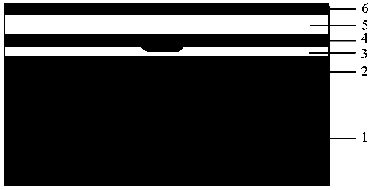
[0019] refer to figure 1 with figure 2 An embodiment of a tunable optical absorber of the present invention is further described.

[0020] In order to achieve the above object, the present invention provides the following technical solutions: a tunable optical absorber, including a substrate 1, the surface of the substrate 1 is deposited in sequence with a lower metal silver film 2, a lower silicon dioxide dielectric film 3, and an n-type antimony film. Indium thin film 4 , upper silicon dioxide dielectric thin film 5 and upper metallic silver thin film 6 .

[0021] Since the resonant frequency of the MIM structure device depends on the dielectric constant, refractive index and thickness of the dielectric material between the two metal materials and other characteristic parameters, the present invention uses the substrate 1 material as the substrate, and its upper surface is a polished surface. , sputtering and other physical vapor deposition techniques deposit the lower me...


PUM

PropertyMeasurementUnit
thicknessaaaaaaaaaa
thicknessaaaaaaaaaa
thicknessaaaaaaaaaa

Abstract

The invention discloses a tunable optical absorber comprising a substrate. A lower metal silver film, a lower silicon dioxide dielectric film, an n type indium antimonide film, an upper silicon dioxide dielectric film and an upper metallic silver film are deposited on the surface of the substrate successively. The invention provides a novel optical absorber being capable of absorbing wavelengths and carrying out dynamic adjustment in real time.

Description

technical field [0001] The invention relates to the field of absorbers, in particular to a tunable light absorber. Background technique [0002] The metal-insulator-metal (MIM) structure is an important spectrally selective absorption device. Due to the metal surface plasmon effect, the structural device will generate a specific plasmon resonance frequency. When the frequency of the incident electromagnetic wave is the same as the resonance frequency of the device, It can produce nearly 100% "perfect absorption". This perfect absorber has broad application prospects in the fields of chemical and biological sensing, solar energy collection, photodetectors, color filters and infrared stealth. [0003] In 2008, Landy et al. first proposed the concept of "perfect absorber" based on the MIM structure (Landy, Phys. Rev. Lett, 2008), which has attracted extensive research. In recent years, by changing the structural size of the micro-nano structure, the arrangement of the units, a...

Claims


Application Information

Patent Timeline
Patent Type & Authority Applications(China)
IPC IPC(8): G02B5/00G02F1/00H01Q17/00
CPCG02B5/003G02F1/0063H01Q17/00
Inventor 谭永胜李秀东
Owner SHAOXING UNIVERSITY
Learn More