A gallium nitride transistor structure and its preparation method

A technology of transistors and gallium nitride, which is applied in semiconductor devices, electrical components, circuits, etc., can solve the problems of small etching options and difficult device processes, and achieve the effects of alleviating electric field concentration, simple growth process, and alleviating virtual gate effects

Active Publication Date: 2022-03-25
安徽长飞先进半导体有限公司 +1
View PDF4 Cites 0 Cited by
  • Summary
  • Abstract
  • Description
  • Claims
  • Application Information

AI Technical Summary

Problems solved by technology

However, due to the relatively small etching selection between p-AlGaN or p-GaN and the epitaxial AlGaN barrier layer, it brings certain difficulties to the device process

Method used


Image

  • A gallium nitride transistor structure and its preparation method
  • A gallium nitride transistor structure and its preparation method
  • A gallium nitride transistor structure and its preparation method

Examples


Embodiment 1

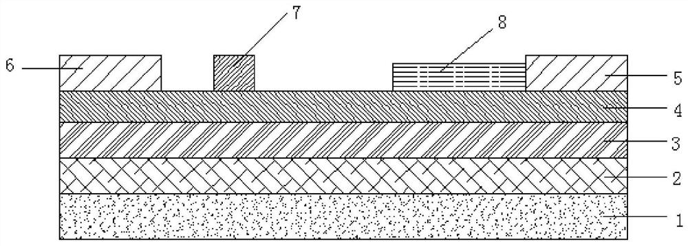
[0040] A gallium nitride transistor structure, comprising a substrate 1, the substrate 1 being a Si, SiC, GaN or sapphire substrate;

[0041] A GaN-based buffer layer 2 located above the substrate 1; a GaN-based channel layer 3 located above the GaN-based buffer layer 2; an In located above the GaN-based channel layer 3 x Al y Ga 1-x-y N barrier layer 4, where 0≤x<1, 0≤y<1, and x+y≠0;

[0042] The structure of the GaN-based buffer layer 2 is, from bottom to top, an AlN nucleation layer, a GaN buffer layer, and an AlGaN buffer layer;

[0043] in In x Al y Ga 1-x-y The source electrode 6 at one end above the N barrier layer 4; the source electrode 6 is an ohmic contact metal electrode, and the ohmic contact metal electrode is composed of a single layer or multiple layers of metal and In x Al y Ga 1-x-y The N barrier layer 4 forms an ohmic contact electrode;

[0044] in In x Al y Ga 1-x-y The drain 5 at the other end above the N barrier layer 4; the drain 5 is an ohmi...

Embodiment 2

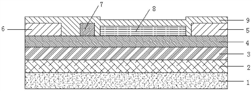
[0055] A gallium nitride transistor structure, the others are the same as in Embodiment 1, except that the uppermost layer of the gallium nitride transistor structure is also covered with a passivation layer 9; the passivation layer 9 includes Si 3 N 4 , Al 2 O 3 , AlN, Y 2 O 3 , La 2 O 3 , Ta 2 O 5 , TiO 2 , HfO 2 , ZrO 2 single-layer or multi-layer composite structures in

[0056] The preparation method of the gallium nitride transistor is the same as in Embodiment 1, except that after step (6), a passivation layer 9 deposition step is included, and the passivation layer 9 is deposited by PECVD, MOCVD, ALD or sputtering.

Embodiment 3

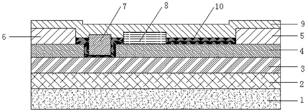
[0058] A gallium nitride transistor structure, comprising a substrate 1, the substrate 1 being a Si, SiC, GaN or sapphire substrate;

[0059] A GaN-based buffer layer 2 located above the substrate 1; a GaN-based channel layer 3 located above the GaN-based buffer layer 2; an In located above the GaN-based channel layer 3 x Al y Ga 1-x-y N barrier layer 4, where 0≤x<1, 0≤y<1, and x+y≠0;

[0060] The structure of the GaN-based buffer layer 2 is, from bottom to top, an AlN nucleation layer, a GaN buffer layer, and an AlGaN buffer layer;

[0061] in In x Al y Ga 1-x-y The source electrode 6 at one end above the N barrier layer 4; the source electrode 6 is an ohmic contact metal electrode, and the ohmic contact metal electrode is composed of a single layer or multiple layers of metal and In x Al y Ga 1-x-y The N barrier layer 4 forms an ohmic contact electrode;

[0062] in In x Al y Ga 1-x-y The drain 5 at the other end above the N barrier layer 4; the drain 5 is an ohmi...


PUM


Abstract

The invention discloses a gallium nitride transistor structure and a preparation method thereof. The gallium nitride transistor structure includes a substrate 1; a GaN-based buffer layer 2 on the substrate 1; an In on the GaN-based buffer layer 2. x al y Ga 1‑x‑y N / GaN heterojunction epitaxial structure; on In x al y Ga 1‑x‑y The source 6 at one end of the surface of the N / GaN heterojunction epitaxial structure; x al y Ga 1‑x‑y The drain 5 at the other end of the surface of the N / GaN heterojunction epitaxial structure; x al y Ga 1‑x‑y The p-type oxide thin film and the gate 7 on the surface of the N / GaN heterojunction epitaxial structure. The present invention is passed in In x al y Ga 1‑x‑y A p-type oxide film is set between the source 6 and the drain 5 on the surface of the N / GaN heterojunction epitaxial structure, and the GaN transistor structure obtained by p-type oxide intercalation can suppress the current collapse effect, and utilize the p-type oxide The holes neutralize the electrons trapped by the surface traps, alleviating the dummy gate effect.

Description

technical field [0001] The invention belongs to the technical field of semiconductors, and in particular relates to a gallium nitride transistor structure and a preparation method thereof. Background technique [0002] Devices based on traditional semiconductor materials such as Si and GaAs are limited by the properties of the materials themselves, so it is difficult to further improve the corresponding indicators of power semiconductor devices. In recent years, the third-generation wide-bandgap semiconductor materials based on group III nitrides have developed rapidly. GaN has excellent material properties such as wide band gap, high saturation electron drift rate, high breakdown field strength and high thermal conductivity, and has great development potential in the fields of high frequency, high temperature, high power and ultraviolet LED. In addition, GaN also has excellent electronic properties, and can form a modulation-doped AlGaN / GaN heterostructure with AlGaN to ob...

Claims


Application Information

Patent Timeline
Patent Type & Authority Patents(China)
IPC IPC(8): H01L29/06H01L29/12H01L29/78
CPCH01L29/0603H01L29/0684H01L29/0611H01L29/2003H01L29/78
Inventor 刘煦冉程海英王敬宋东波
Owner 安徽长飞先进半导体有限公司
Why Eureka
Try Eureka