A high breakdown voltage GaN-based high electron mobility transistor

A technology of electron mobility and high breakdown voltage, which is applied in the direction of circuits, electrical components, semiconductor devices, etc., to achieve the effect of solving the problem of low breakdown voltage and good thermal stability

Active Publication Date: 2018-04-24
南京绿能芯耀科技有限公司
View PDF3 Cites 0 Cited by
  • Summary
  • Abstract
  • Description
  • Claims
  • Application Information

AI Technical Summary

Problems solved by technology

[0007] The technical problem to be solved by the present invention is to provide a high breakdown voltage GaN-based high electron mobility solution that can avoid the problems of charge imbalance and poor thermal stability, and can improve its own breakdown voltage. transistor

Method used


Image

  • A high breakdown voltage GaN-based high electron mobility transistor
  • A high breakdown voltage GaN-based high electron mobility transistor
  • A high breakdown voltage GaN-based high electron mobility transistor

Examples


Embodiment Construction

[0026]The present invention will be further described in detail below in conjunction with the accompanying drawings and embodiments.

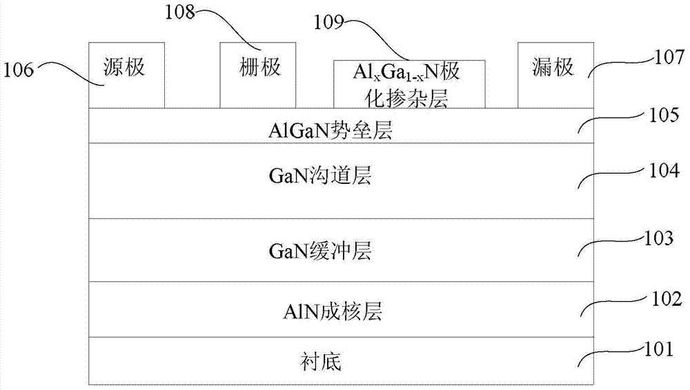
[0027] Such as figure 2 As shown, the GaN-based high electron mobility transistor with high breakdown voltage in this embodiment mainly consists of substrate 101, AlN nucleation layer 102, GaN buffer layer 103, GaN channel layer 104, AlGaN barrier layer 105, and the source 106, drain 107 and gate 108 formed on the AlGaN barrier layer 105, as an improvement, the GaN-based high electron mobility transistor also includes an AlGaN barrier layer 105 and between the gate 108 and the drain 107 is formed with an Al composition gradient Al x Ga 1-x N-polarized doped layer 109 .

[0028] Al in this example x Ga 1-x The thickness of the N-polarized doped layer 109 is between 50nm and 500nm, and the Al x Ga 1-x The Al composition on the upper surface of the N-polarized doped layer 109 is 0, and the Al composition on the lower surface is the same as...


PUM


Abstract

The invention relates to a high-breakdown-voltage GaN-based high-electron-mobility transistor, which mainly comprises a substrate, an AlN nucleation layer, a GaN buffer layer, a GaN channel layer, a AlGaN barrier layer, a source electrode, a drain electrode and a grid electrode, wherein the above layers are successively arranged from bottom to top and the source electrode, the drain electrode and the grid electrode are formed on the AlGaN barrier layer. The high-breakdown-voltage GaN-based high-electron-mobility transistor is characterized by further comprising an AlxGa1-xN polarization doped layer positioned on the AlGaN barrier layer and between the grid electrode and the drain electrode, with the content of Al component to be gradually changed. The content of Al component in the AlxGa1-xN polarization doped layer is linearly increased from top to bottom. The three-dimensional hole gas generated caused by he gradually changing content of Al component and the two-dimensional electron gas of the channel layer compensate each other to form a charge self-balancing type super-junction structure. In this way, the charge imbalance problem is solved. Meanwhile, the breakdown voltage and the stability of equipment are improved.

Description

technical field [0001] The invention relates to the field of semiconductor devices, in particular to a gallium nitride-based high electron mobility transistor with high breakdown voltage. Background technique [0002] Gallium nitride (GaN)-based high electron mobility transistor (HEMT) not only has excellent characteristics such as large band gap, high critical breakdown electric field, high electron saturation velocity, good thermal conductivity, radiation resistance and good chemical stability, but also nitrogen Gallium nitride (GaN) materials can also form two-dimensional electron gas (2DEG) heterojunction channels with high concentration and high mobility with materials such as aluminum gallium nitride (AlGaN). Therefore, gallium nitride (GaN)-based high electron mobility transistors are especially suitable for high-voltage, high-power and high-temperature applications, and are one of the most potential transistors for power electronics applications. [0003] However, t...

Claims


Application Information

Patent Timeline
Patent Type & Authority Patents(China)
IPC IPC(8): H01L29/778H01L29/06
CPCH01L29/0603H01L29/7787
Inventor 赵子奇桂进争周幸叶姜涛张后程胡子阳
Owner 南京绿能芯耀科技有限公司
Why Eureka
Try Eureka