GaN MISHEMT device and manufacturing method thereof

A fabrication method and technology of a barrier layer, applied in the fields of semiconductor/solid-state device manufacturing, semiconductor devices, electrical components, etc., can solve the problems of affecting the threshold voltage of devices, restricting commercial applications, and deteriorating device yields, and achieving good DC Characteristics and dynamic characteristics, suppression of current collapse effect, effect of excellent electrical insulation properties

Pending Publication Date: 2021-11-02
SUZHOU INST OF NANO TECH & NANO BIONICS CHINESE ACEDEMY OF SCI
View PDF0 Cites 0 Cited by
  • Summary
  • Abstract
  • Description
  • Claims
  • Application Information

AI Technical Summary

Problems solved by technology

Although GaN HEMT devices have many advantages, their commercial application has been limited by reliability issues, gate leakage issues, and current collapse effects.
However, the preparation of these GaN MISHEMT dielectric layers is usually transferred to other equipment for secondary epitaxy after the growth of the HEMT epitaxial structure is completed, which will inevitably be affected by the environment and process. The gap between the dielectric layer and (Al)GaN A new interface state is brought between them, so that the MISHEMT device cannot effectively suppress the current collapse effect, which leads to the deterioration of the dynamic characteristics of the device
[0004] see figure 1 , the prior art discloses the technical scheme of using h-BN as a single dielectric layer or inserting h-BN between AlGaN and the dielectric layer to passivate the surface of the HEMT device. However, the h in the MISHEMT device disclosed in the prior art -BN is prepared by transfer or secondary deposition after the growth of the HEMT epitaxial structure is completed. Because of the two-dimensional characteristics of h-BN, h-BN as a single dielectric layer has the problem of poor bonding with GaN, so in It is easy to fall off during the process, which will cause the yield of the device to deteriorate. In addition, if this structure is prepared by transfer or secondary deposition, it will inevitably be affected by the environment and process and cause a band between h-BN and AlGaN. A new interface state will come, which will affect the performance of the device, and the current collapse effect cannot be effectively suppressed, making the dynamic characteristics of the device worse.
[0005] In addition, some researchers have used in-situ growth of SiN to passivate the surface of AlGaN, but SiN does not have two-dimensional characteristics, and the fixed charge at the interface between SiN and h-BN will seriously affect the threshold voltage of the device

Method used


Image

  • GaN MISHEMT device and manufacturing method thereof
  • GaN MISHEMT device and manufacturing method thereof
  • GaN MISHEMT device and manufacturing method thereof

Examples


Embodiment Construction

[0021] In view of the deficiencies in the prior art, the inventor of this case was able to propose the technical solution of the present invention after long-term research and extensive practice. The technical solution, its implementation process and principle will be further explained as follows.

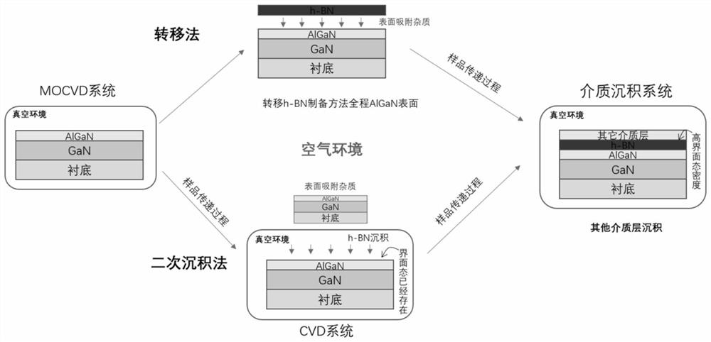
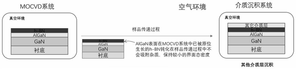
[0022] The methods for making h-BN in the prior art mainly include: solid phase reaction method, microwave molten salt method and chemical vapor deposition (CVD) etc. (see Cui Shiqiang, Kan Hongmin, Zhang Ning, and Ru Hongqiang, "Hexagonal Nitrogen Preparation, application and research progress of boron oxide, "Functional Materials, vol.51, no.08, pp.8072-8077, 2020), people have formed an inherent cognition with inertial thinking, and try to prepare h-BN by different methods And transferred to prepare HEMT, but did not fully realize that the interface state introduced in the transfer process will not only not effectively play the role of h-BN, but will affect a series of device pe...


PUM

PropertyMeasurementUnit
thicknessaaaaaaaaaa
thicknessaaaaaaaaaa

Abstract

The invention discloses a GaN MISHEMT device and a manufacturing method thereof. The manufacturing method comprises the steps that an epitaxial structure is manufactured, the epitaxial structure comprises a channel layer and a barrier layer formed on the channel layer, and two-dimensional electron gas is formed between the AlGaN barrier layer and the channel layer; a two-dimensional material passivation layer epitaxially is grown on the barrier layer in situ; a dielectric layer is formed on the two-dimensional material passivation layer; a source electrode, a drain electrode and a grid electrode are manufactured, the source electrode and the drain electrode are arranged on the barrier layer and electrically connected through the two-dimensional electron gas, and the grid electrode is arranged on the dielectric layer and located between the source electrode and the drain electrode. According to the manufacturing method provided by the invention, after the GaN HEMT epitaxial structure is grown, the two-dimensional h-BN is grown in situ to serve as the surface passivation layer, and then the dielectric layer is deposited for the second time, so that surface damage can be blocked, surface dangling bonds can be shielded, the interface state density can be reduced, the current collapse effect can be effectively inhibited, and the device can obtain better direct current characteristics and dynamic characteristics.

Description

technical field [0001] The invention relates to a HEMT device, in particular to a GaN MISHEMT device and a manufacturing method thereof, belonging to the technical field of semiconductors. Background technique [0002] Since the 21st century, global climate warming has become prominent, environmental pollution has become serious, and the energy crisis has intensified. How to realize efficient and environmentally friendly energy utilization becomes the key to improving these problems. As one of the most important energy sources for human beings, electric energy consumes a lot in social production and life. Therefore, improving the conversion efficiency of power conversion systems is very important to reduce the waste of electric energy. GaN HEMT devices are very suitable for high-frequency, high-temperature and high-power applications, such as wireless communication base stations, radar, automotive electronics, and power grid transmission, due to their excellent characteristi...

Claims


Application Information

Patent Timeline
Patent Type & Authority Applications(China)
IPC IPC(8): H01L21/335H01L29/778
CPCH01L29/66462H01L29/7786
Inventor 于子呈张丽周鑫徐坤邓旭光范亚明张宝顺
Owner SUZHOU INST OF NANO TECH & NANO BIONICS CHINESE ACEDEMY OF SCI
Why Eureka
Try Eureka