A p-type buried layer algan-gan high electron mobility transistor

A high electron mobility, transistor technology, applied in circuits, electrical components, semiconductor devices, etc., can solve problems such as the decline of the current capacity of the device, reduce the concentration of 2DEG in the device, and achieve the effect of suppressing the current collapse effect.

Active Publication Date: 2019-04-30
SOUTHEAST UNIV
View PDF2 Cites 0 Cited by
  • Summary
  • Abstract
  • Description
  • Claims
  • Application Information

AI Technical Summary

Problems solved by technology

The existing methods of increasing the barrier height of the AlN nucleation layer, such as increasing the Al composition of the AlN nucleation layer, can effectively suppress the current collapse effect, but at the same time, this method will reduce the 2DEG concentration of the device, which will reduce the current capability of the device

Method used


Image

  • A p-type buried layer algan-gan high electron mobility transistor
  • A p-type buried layer algan-gan high electron mobility transistor
  • A p-type buried layer algan-gan high electron mobility transistor

Examples


Embodiment Construction

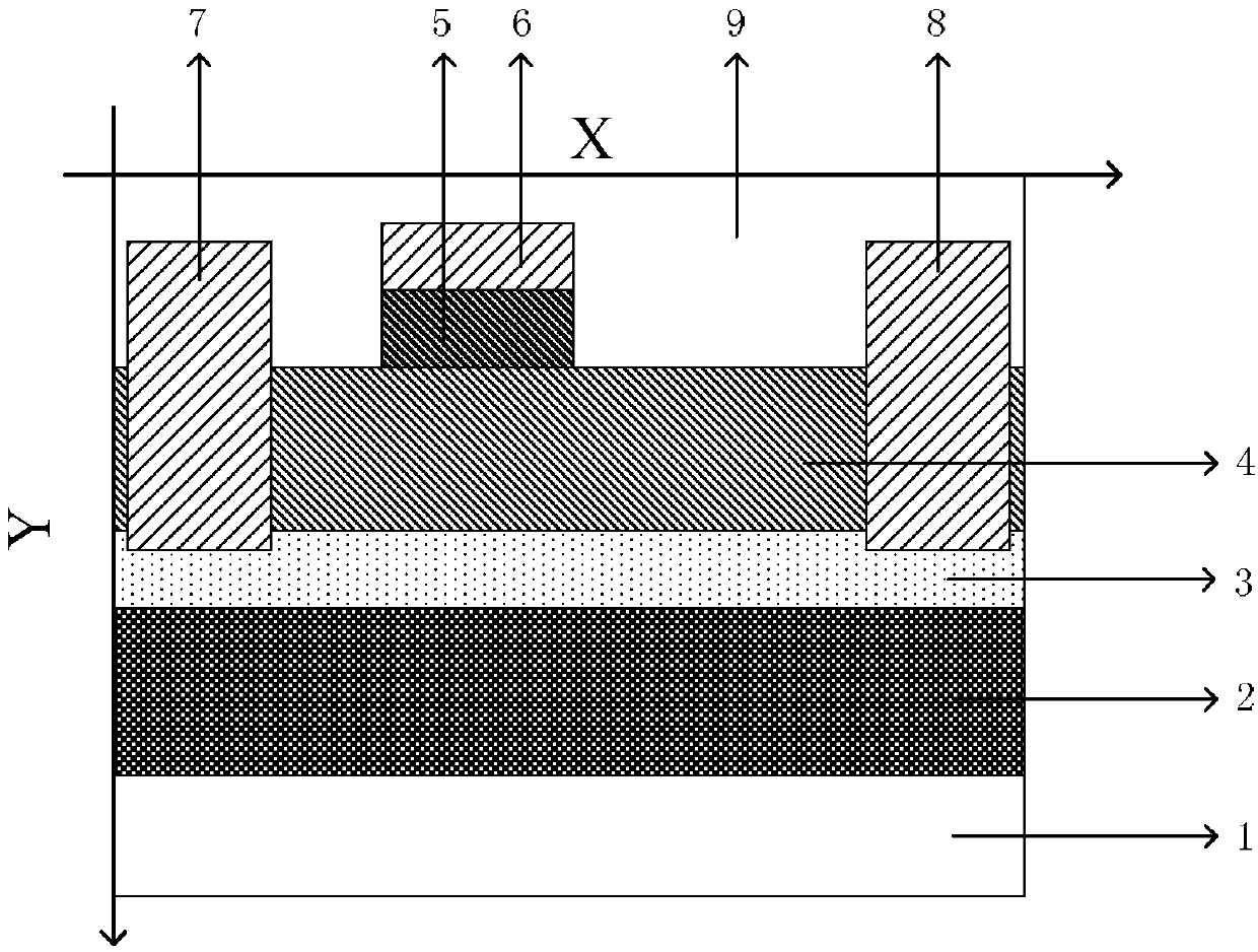
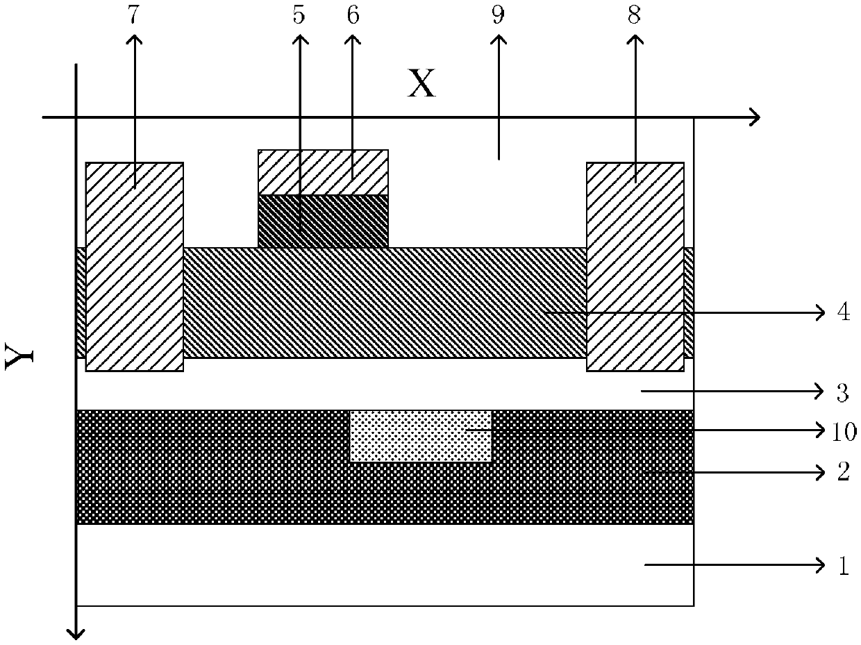
[0015] A P-type buried layer AlGaN-GaN high electron mobility transistor, comprising: a Si-based substrate 1, an AlN nucleation layer 2 is formed on the Si-based substrate 1, and an intrinsic GaN is formed on the AlN nucleation layer 2 layer 3, an AlGaN doped layer 4 is formed on the intrinsic GaN layer 3, a gate oxide layer 5 is formed on the upper surface of the AlGaN doped layer 4, a gate 6 is formed on the upper surface of the gate oxide layer 5, and the AlGaN doped The impurity layer 4 and the gate 6 are covered with a passivation layer 9, and a source 7 is formed on one side of the gate 6, the source 7 starts from the upper part of the intrinsic GaN layer 3, penetrates the AlGaN doped layer 4 and ends In the passivation layer 9, a drain 8 is formed on the other side of the gate 6, the drain 8 starts from the upper part of the intrinsic GaN layer 3, passes through the AlGaN doped layer 4 and ends in the passivation layer 9, It is characterized in that a P-type AlGaN doped...


PUM


Abstract

An AlGaN-GaN high-electron mobility transistor with a P-type buried layer comprises a Si-based substrate, wherein an AlN nucleating layer is formed on the Si-based substrate, an intrinsic GaN layer is formed on the AlN nucleating layer, an AlGaN doping layer is formed on the intrinsic GaN layer, a gate oxide layer is formed on an upper surface of the AlGaN doping layer, a gate is formed on an upper surface of the gate oxide layer, a passivation layer covers the AlGaN doping layer and the gate, a source is formed at one side of the gate, a drain is formed at the other side of the gate, the source and the drain extend form an upper part of the intrinsic GaN layer, penetrate through the AlGaN doping layer and are stopped in the passivation layer, the AlGaN-GaN high-electron mobility transistor is characterized in that a P-type AlGaN doping region buried layer is formed in the AlN nucleating layer, an upper surface of the P-type AlGaN doping region buried layer is in contact with a lower surface of the intrinsic GaN layer, a boundary of the P-type AlGaN doping region buried layer is arranged below the gate, and the other boundary of the P-type AlGaN doping region buried layer is arranged below a region between the gate and the drain.

Description

technical field [0001] The invention mainly relates to a wide bandgap material power semiconductor device, in particular to an AlGaN-GaN high electron mobility transistor used in the field of power switches. Background technique [0002] GaN material has good electrical properties, such as wide band gap, high breakdown electric field, high thermal conductivity, corrosion resistance, etc. The third-generation semiconductor material after the material is an ideal material for making high-frequency, high-voltage, high-temperature, high-power electronic devices and short-wavelength, high-power optoelectronic devices. [0003] AlGaN-GaN high electron mobility transistor Due to the spontaneous polarization effect, a high concentration of two-dimensional electron gas (2DEG) appears in the GaN layer at the AlGaN-GaN interface, so the AlGaN-GaN high electron mobility transistor has an electron drift speed Fast advantage. Since the AlGaN-GaN high electron mobility transistor also ha...

Claims


Application Information

Patent Timeline
Patent Type & Authority Patents(China)
IPC IPC(8): H01L29/778H01L29/06
CPCH01L29/0684H01L29/7786
Inventor 孙伟锋陈欣魏家行杨翰琪任晓飞刘斯扬陆生礼时龙兴
Owner SOUTHEAST UNIV
Why Eureka
Try Eureka