

A gan heterojunction field effect transistor with low junction temperature and high withstand voltage
A heterojunction field effect, high withstand voltage technology, used in transistors, semiconductor devices, electric solid devices, etc., can solve problems such as accelerated electromigration, reliability problems, and damage to connecting die wires.
Active Publication Date: 2021-08-17
UNIV OF ELECTRONICS SCI & TECH OF CHINA
View PDF4 Cites 0 Cited by
- Summary
- Abstract
- Description
- Claims
- Application Information
AI Technical Summary
Problems solved by technology
Self-heating effects can accelerate electromigration, degrade the gate, and can damage the wires connecting the die to the package case, causing a series of reliability problems
Method used
View moreImage
Smart ImageViewing Examples

Examples
Embodiment Construction
[0036] The technical solution of the present invention has been described in detail in the part of the content of the invention, and will not be repeated here.
Login to View More PUM
| Property | Measurement | Unit |
|---|---|---|
| thickness | aaaaa | aaaaa |
| thickness | aaaaa | aaaaa |
| thickness | aaaaa | aaaaa |
Abstract
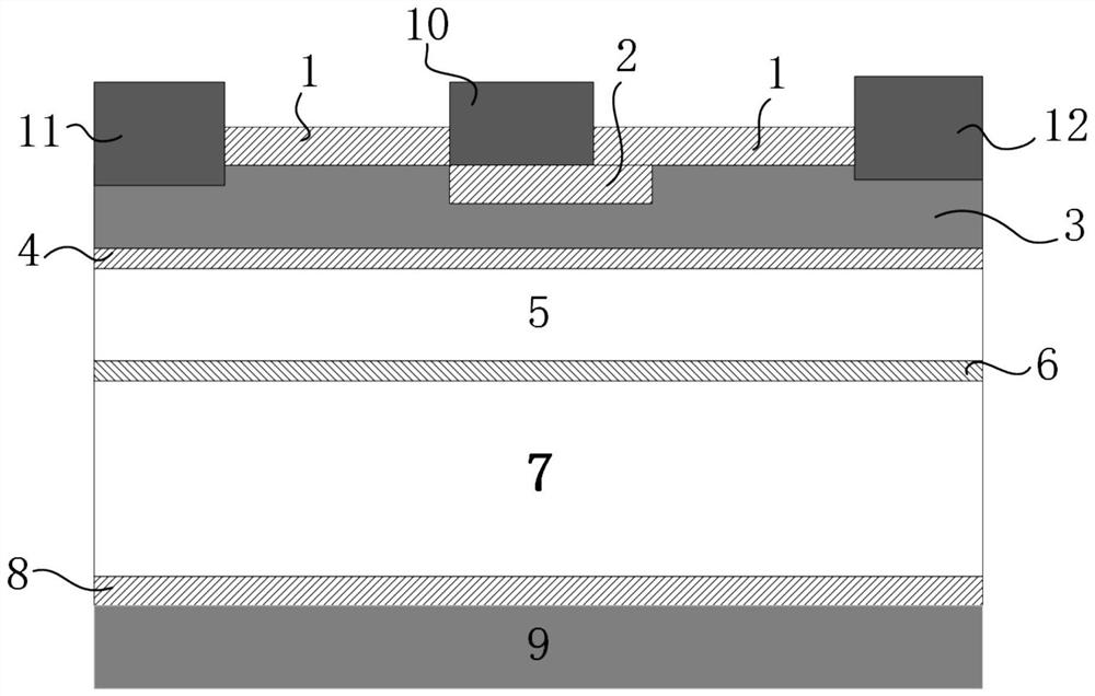
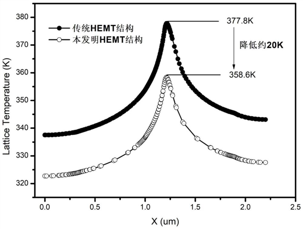
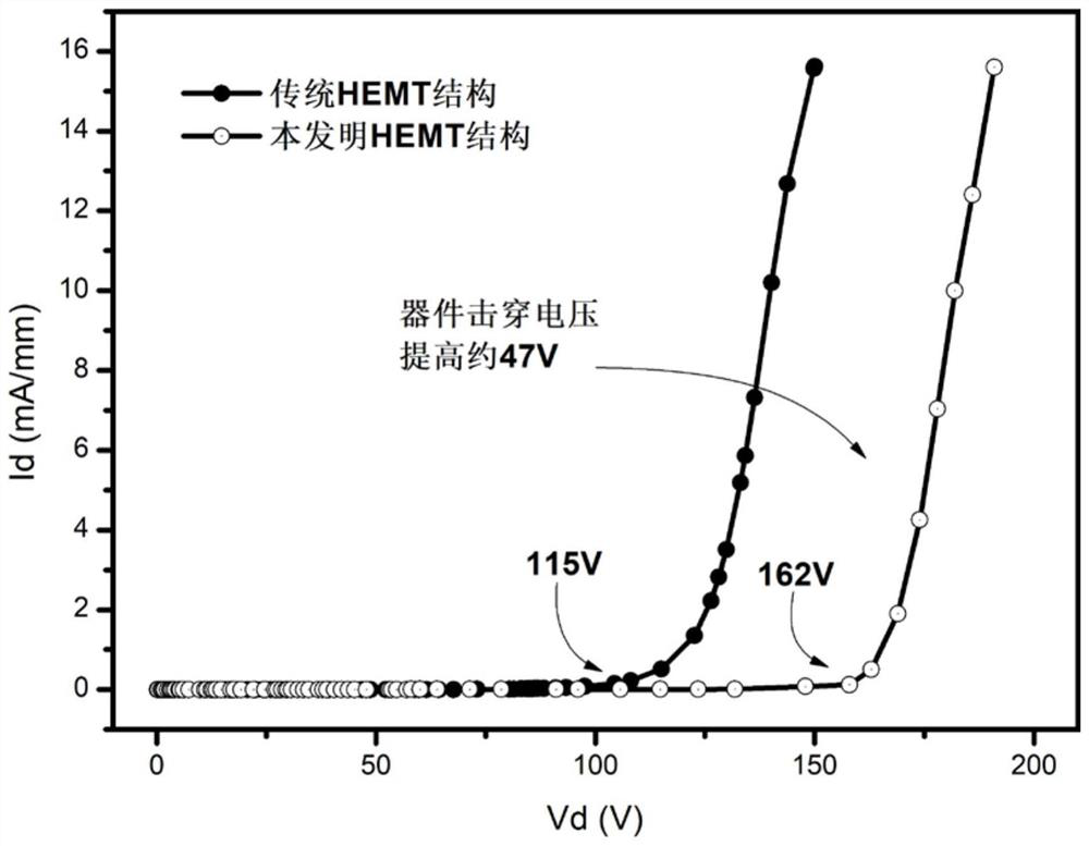
The invention designs power semiconductor technology, specifically a GaN heterojunction field effect transistor with low junction temperature and high withstand voltage. The GaN heterojunction field effect transistor of the present invention mainly lowers the peak electric field of the channel by inserting an AlN region in the barrier layer, thereby achieving the purpose of increasing withstand voltage and reducing heat dissipation. In addition, the present invention uses AlN with good thermal conductivity as the passivation layer of the device, which not only helps to suppress current collapse, but also accelerates heat dissipation. The excellent effect of the invention is that the reverse withstand voltage of the device is improved, the output characteristics of the device are improved, and the channel temperature of the device is reduced, thereby suppressing the harm caused by the current collapse and the self-heating effect. The invention is especially suitable for GaN heterojunction field effect transistors with high withstand voltage capability and low channel temperature.
Description
technical field [0001] The invention belongs to the technical field of power semiconductors, and relates to a GaN heterojunction field effect transistor with low junction temperature and high withstand voltage. Background technique [0002] With the advancement of science and technology, the demand for electric energy in human society is increasing day by day. How to efficiently use electric energy has become a problem that has to be considered at present. At present, almost all electrical energy must be converted by power semiconductor devices before it can be used by electronic equipment. As one of the foundation and core technologies of new energy and energy conservation and emission reduction, power semiconductor technology has effectively promoted the application of electric energy in a more efficient, energy-saving and environmentally friendly manner. In recent years, with the rise of new energy vehicles and other fields, power semiconductor technology has a broader a...
Claims
Login to View More Application Information
Patent Timeline
 Patent Type & AuthorityPatents(China)
IPC IPC(8): H01L29/06H01L29/10H01L29/20H01L29/778H01L23/373
CPCH01L23/3738H01L29/0615H01L29/0684H01L29/1029H01L29/2003H01L29/7787
Inventor陈万军李佳肖立杨李茂林信亚杰施宜军
OwnerUNIV OF ELECTRONICS SCI & TECH OF CHINA