

Source bottle used for thin film deposition equipment and semiconductor equipment
A thin film deposition and source bottle technology, applied in gaseous chemical plating, metal material coating process, coating, etc., can solve problems such as solid source condensation, and achieve simplified sealing design, improved space utilization, and uniform temperature distribution Effect
- Summary
- Abstract
- Description
- Claims
- Application Information
AI Technical Summary
Problems solved by technology
Method used
Image

Examples
Embodiment
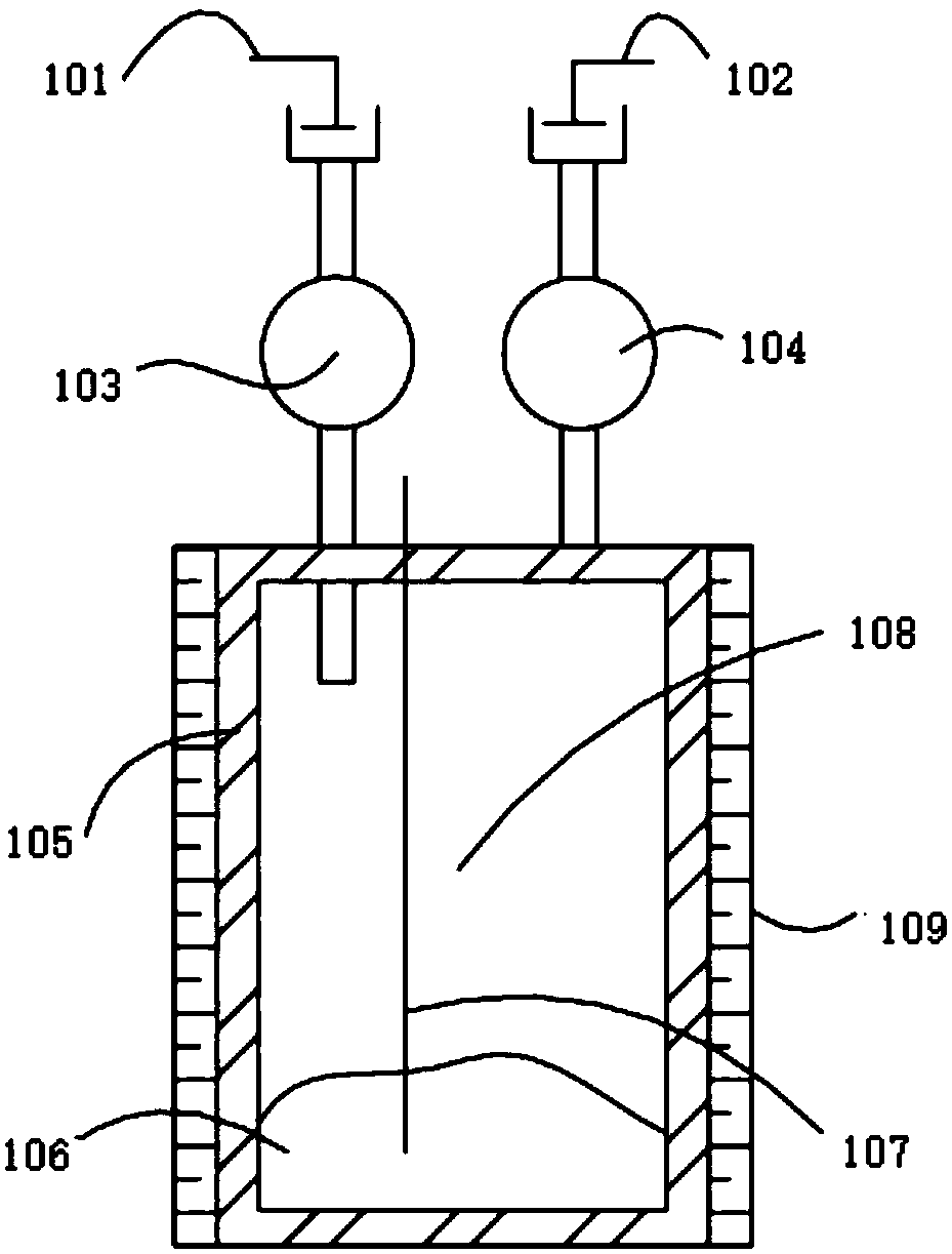
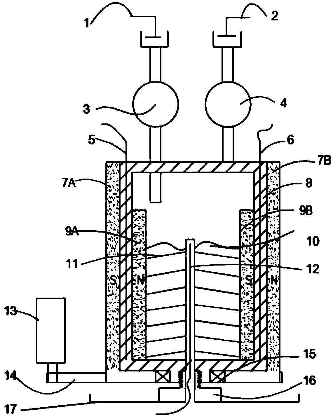
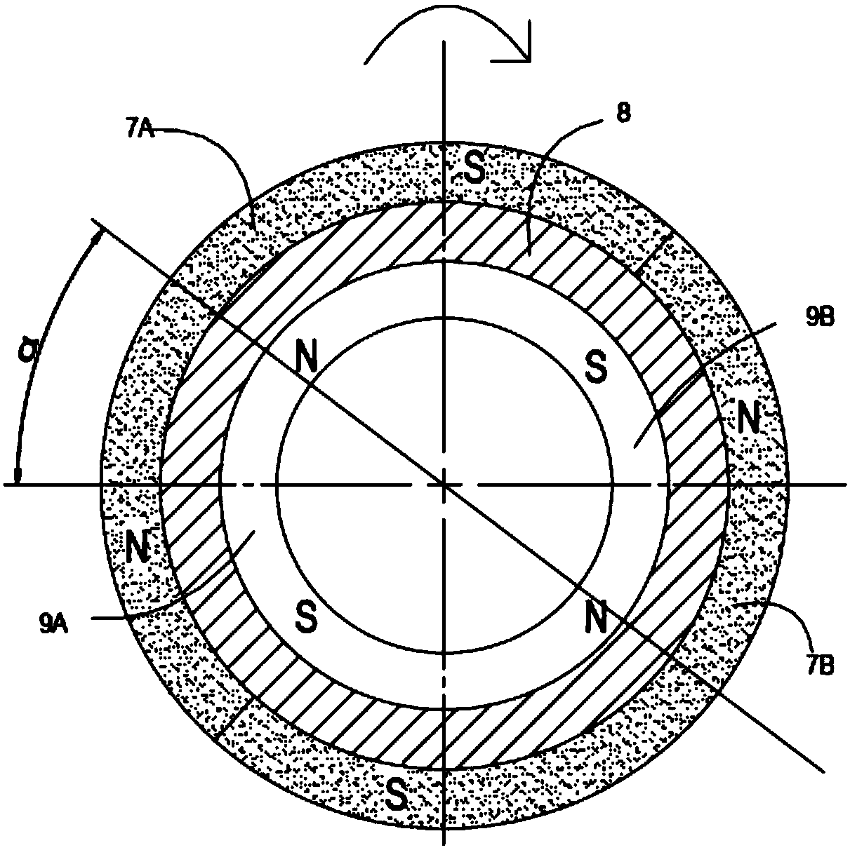
[0056] figure 2 with image 3 respectively showing a longitudinal sectional view and a transverse sectional view of a source bottle for a thin film deposition apparatus according to an exemplary embodiment of the present invention, Figure 4 A partial longitudinal sectional view showing a source bottle for a thin film deposition apparatus according to an exemplary embodiment of the present invention, Figure 5 A longitudinal sectional view showing a carrier of a source bottle for a thin film deposition apparatus according to an exemplary embodiment of the present invention.
[0057] Such as Figure 2-5 As shown, the source bottle used for thin film deposition equipment according to the exemplary embodiment includes a source bottle body 8, an internal rotating member arranged in the source bottle body 8 and connected to it, and a carrier 11 for carrying a solid state source 10. Based on the outer rotating part outside the source bottle body 8 and the drive motor 13 for driv...
PUM
 Abstract
Description
Claims
Application Information