High-temperature pressure sensor chip based on MEMS process

A pressure sensor and chip technology, applied in the measurement of the elastic deformation force of the measurement gauge, the measurement of the property force of the applied piezoelectric resistance material, etc., can solve the problems of piezoresistive element and metal layer connection failure, metal fracture, etc. Achieve good high temperature resistance and stability, not easy to oxidize, and avoid oxidation failure

Inactive Publication Date: 2019-11-19
TSINGHUA UNIV
View PDF6 Cites 4 Cited by
  • Summary
  • Abstract
  • Description
  • Claims
  • Application Information

AI Technical Summary

Problems solved by technology

[0006] The purpose of the present invention is to provide a high-temperature pressure sensor chip based on MEMS technology to solve the problems caused by the loss of thermal expansion coefficient between the chip base, the piezoresistive element and the metal layer under high temperature conditions. Problems such as metal fracture caused by matching, piezoresistive element and metal layer connection failure, etc., so as to further improve its high temperature resistance and stability, and effectively measure gas-liquid pressure under high temperature conditions

Method used


Image

  • High-temperature pressure sensor chip based on MEMS process
  • High-temperature pressure sensor chip based on MEMS process

Examples


Embodiment Construction

[0017] The present invention will be further described below in conjunction with the accompanying drawings and embodiments, so that those skilled in the art can fully understand and realize the present invention.

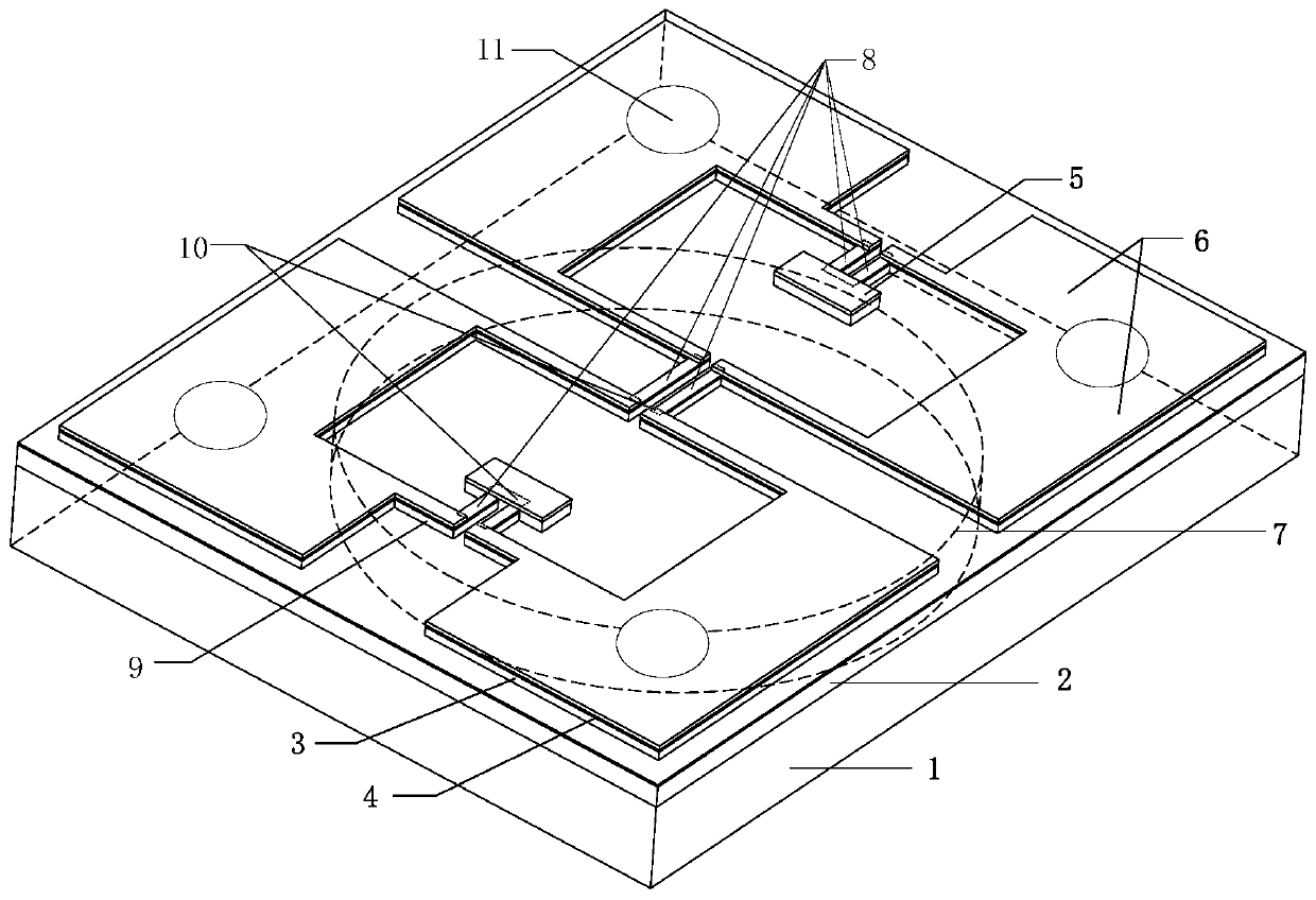
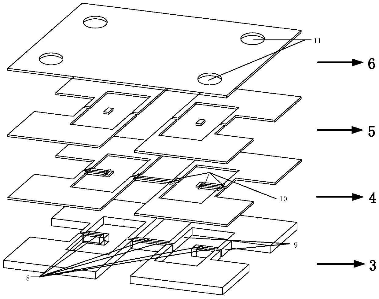
[0018] figure 1 It is a structural schematic diagram of a MEMS-based high-temperature pressure sensor chip involved in the present invention. The high-temperature pressure sensor chip includes a chip base 1, a P-type epitaxial layer 2, an N-type epitaxial layer 3, a piezoresistive element isolation layer 4, a metal layer 5, and a pressure-sensitive film 7; the N-type epitaxial layer 3 includes a piezoresistive The element 8 and the connecting bracket 9 have the same thickness; the piezoresistive element isolation layer 4 covers the piezoresistive element 8 and the connecting bracket 9, and the position corresponding to the piezoresistive element 8 is etched on the piezoresistive element isolation layer There is an ohmic contact window 10; the metal layer and the pi...


PUM

PropertyMeasurementUnit
Thicknessaaaaaaaaaa
Thicknessaaaaaaaaaa
Thicknessaaaaaaaaaa

Abstract

The invention discloses a high-temperature pressure sensor chip based on an MEMS process. The high-temperature pressure sensor chip comprises a chip base, a P-type epitaxial layer, an N-type epitaxiallayer, a pressure-sensitive thin film, a piezoresistive element, a connection support, a piezoresistive element isolation layer, an ohmic contact window, a metal layer and a metal layer protective layer, wherein the obverse side of the chip base bears the piezoresistive element; the pressure-sensitive thin film is formed on the reverse side of the chip base in an etched mode; the piezoresistive element and the connection support are formed on the N-type epitaxial layer in an etched mode; the piezoresistive element isolation layer covers the piezoresistive element and the connection support; the metal layer and the piezoresistive element are connected with each other through the ohmic contact window etched in the piezoresistive element isolation layer; and the connection height between thepiezoresistive element and the metal layer is the thickness of the piezoresistive element isolation layer. The pressure sensor chip not only can work stably in a high-temperature environment but alsoeffectively avoids the problem of oxidation failure of the piezoresistive element and the metal layer, thereby having a broad application prospect.

Description

technical field [0001] The invention relates to a high-temperature pressure sensor based on MEMS processes such as epitaxial doping, wet etching, and ICP etching, and belongs to the technical field of design and manufacture of pressure sensors. Background technique [0002] Sensor technology is an important symbol of the development level of modern science and technology, and pressure sensors are the most widely used type of sensors. [0003] Traditional pressure sensors are mainly based on mechanical structural devices, and the deformation of elastic elements is used to indicate pressure, but this structure is large in size and heavy in weight, and cannot provide electrical output. With the development of semiconductor technology and MEMS technology, people use silicon as the main material to develop silicon micro pressure sensors. It is characterized by small size, light weight, high accuracy and good temperature characteristics. The current semiconductor pressure sensor...

Claims


Application Information

Patent Timeline
IPC IPC(8): G01L1/18G01L1/04
CPCG01L1/04G01L1/18
Inventor 唐飞刘海冰谭庆尹德帅王晓浩
Owner TSINGHUA UNIV
Why Eureka
Try Eureka