OLED display substrate and manufacturing method thereof, and display device

A technology for display substrates and manufacturing methods, which is applied in the field of OLED displays, can solve the problems of micro mobile display devices that cannot be displayed normally, and metal wires fall off, and achieve the effects of reducing the risk of metal wire falling off, wear resistance and high strength

Active Publication Date: 2019-11-19
BOE TECH GRP CO LTD
View PDF4 Cites 11 Cited by
  • Summary
  • Abstract
  • Description
  • Claims
  • Application Information

AI Technical Summary

Problems solved by technology

In order to apply the OLED display panel to the micro mobile display device, the OLED display panel and the external circuit are bonded together by a wire bonding process to effectively reduce the size of the micro mobile display device, but due to the wire bonding used The metal traces are relatively thin, so there is a risk of falling off the metal traces used for the wire bonding between the OLED display panel and the external circuit, resulting in the failure of the micro mobile display device to display normally

Method used


Image

  • OLED display substrate and manufacturing method thereof, and display device
  • OLED display substrate and manufacturing method thereof, and display device
  • OLED display substrate and manufacturing method thereof, and display device

Examples


Embodiment Construction

[0028] The following will clearly and completely describe the technical solutions in the embodiments of the present invention with reference to the accompanying drawings in the embodiments of the present invention. Obviously, the described embodiments are only some, not all, embodiments of the present invention. Based on the embodiments of the present invention, all other embodiments obtained by persons of ordinary skill in the art without creative efforts fall within the protection scope of the present invention.

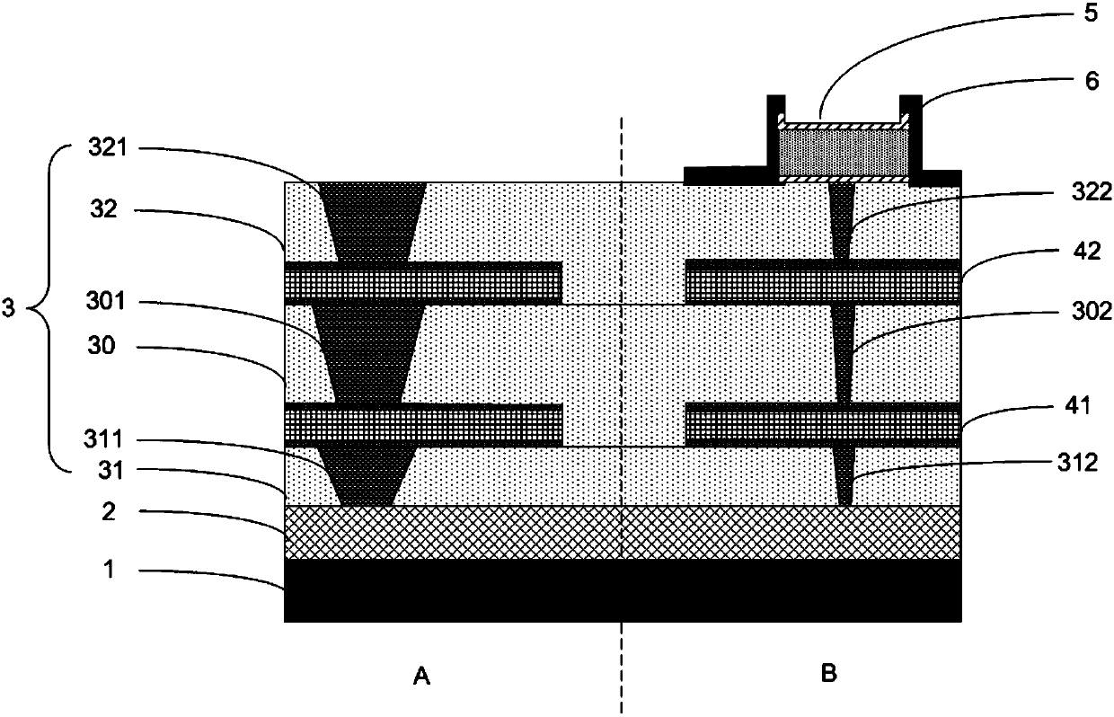
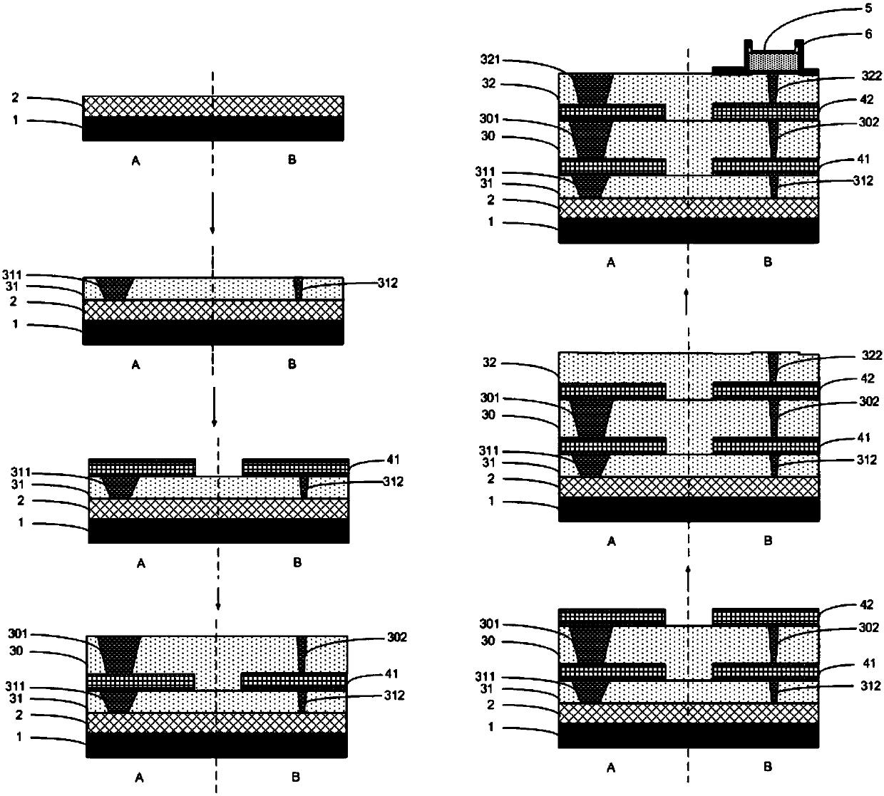
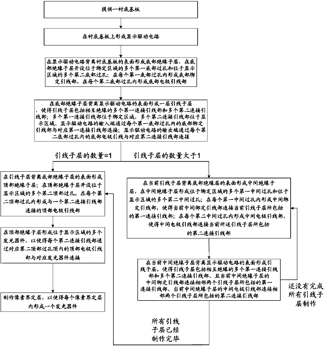
[0029] see figure 1 , the OLED display substrate provided by the embodiment of the present invention includes a binding area A and a display area B, the binding area A includes a plurality of first signal via holes providing binding lead channels, and the display area B includes a plurality of first signal via holes providing electrode lead channels For the second signal via hole, the aperture diameters of the plurality of first signal via holes are all larger than...


PUM


Abstract

The invention discloses an OLED display substrate and a manufacturing method thereof, and a display device, relates to the technical field of OLED display, and aims to reduce the risk that metal wiresused for wire binding between an OLED display panel and an external circuit fall off. The OLED display substrate comprises a binding area and a display area. The binding area comprises a plurality offirst signal via holes for providing binding lead channels, the display area comprises a plurality of second signal via holes for providing electrode lead channels, and the aperture of each of the plurality of first signal via holes is larger than that of each of the plurality of second signal via holes. The manufacturing method of the OLED display substrate is used for manufacturing the OLED display substrate. The OLED display substrate and the manufacturing method of the OLED display substrate and the display device are used in the display technology.

Description

technical field [0001] The invention relates to the field of OLED display technology, in particular to an OLED display substrate, a manufacturing method thereof, and a display device. Background technique [0002] At present, the pictures displayed by micro mobile display devices based on technologies such as virtual reality (Virtual Reality, abbreviated as VR) and augmented display (Augmented Reality, abbreviated as AR) need to meet the characteristics of high resolution, high brightness, and high contrast, so as to meet Demand for miniature mobile display devices. [0003] In the prior art, most micro mobile display devices use OLED display panels with self-luminous performance to display pictures, so that the pictures displayed by the micro mobile display devices meet low afterglow during movement, so as to reduce the user's sense of dizziness. In order to apply the OLED display panel to the micro mobile display device, the OLED display panel and the external circuit are...

Claims


Application Information

Patent Timeline
Patent Type & Authority Applications(China)
IPC IPC(8): H01L27/32H01L51/56
CPCH10K59/131H10K59/123H10K59/124H10K59/80517H10K71/231H10K50/81H10K50/82H10K59/121H10K59/122H10K71/00H10K2102/311
Inventor 王维海陈小川杨盛际卢鹏程
Owner BOE TECH GRP CO LTD
Why Eureka
Try Eureka