Anti-welding method for small aperture through holes

A small-aperture, anti-soldering technology, which is applied in the fields of printed circuit manufacturing, cleaning/polishing of conductive patterns, and secondary treatment of printed circuits, can solve problems such as large quality risks, ink entering holes, and affecting the first pass rate, etc., to increase Light curing effect, the effect that meets the production demand

Inactive Publication Date: 2019-11-19
江西景旺精密电路有限公司
View PDF5 Cites 1 Cited by
  • Summary
  • Abstract
  • Description
  • Claims
  • Application Information

AI Technical Summary

Problems solved by technology

[0002] At present, the production method of solder mask through holes in the PCB industry is generally produced by spraying and dot printing. For holes designed with a window opening of ≤4mil (1mil=25.4μm), the above two methods will cause the problem of ink entering the hole
In addition, the ink hole problem has always been a common problem for solder mask, which affects the first pass rate and has a great quality risk, which cannot meet the production demand

Method used


Image

  • Anti-welding method for small aperture through holes

Examples


Embodiment Construction

[0025] The following will clearly and completely describe the technical solutions in the embodiments of the present invention with reference to the accompanying drawings in the embodiments of the present invention. Obviously, the described embodiments are some of the embodiments of the present invention, but not all of them. Based on the embodiments of the present invention, all other embodiments obtained by persons of ordinary skill in the art without making creative efforts belong to the protection scope of the present invention.

[0026] It should be understood that when used in this specification and the appended claims, the terms "comprising" and "comprises" indicate the presence of described features, integers, steps, operations, elements and / or components, but do not exclude one or Presence or addition of multiple other features, integers, steps, operations, elements, components and / or collections thereof.

[0027] It should also be understood that the terminology used ...


PUM


Abstract

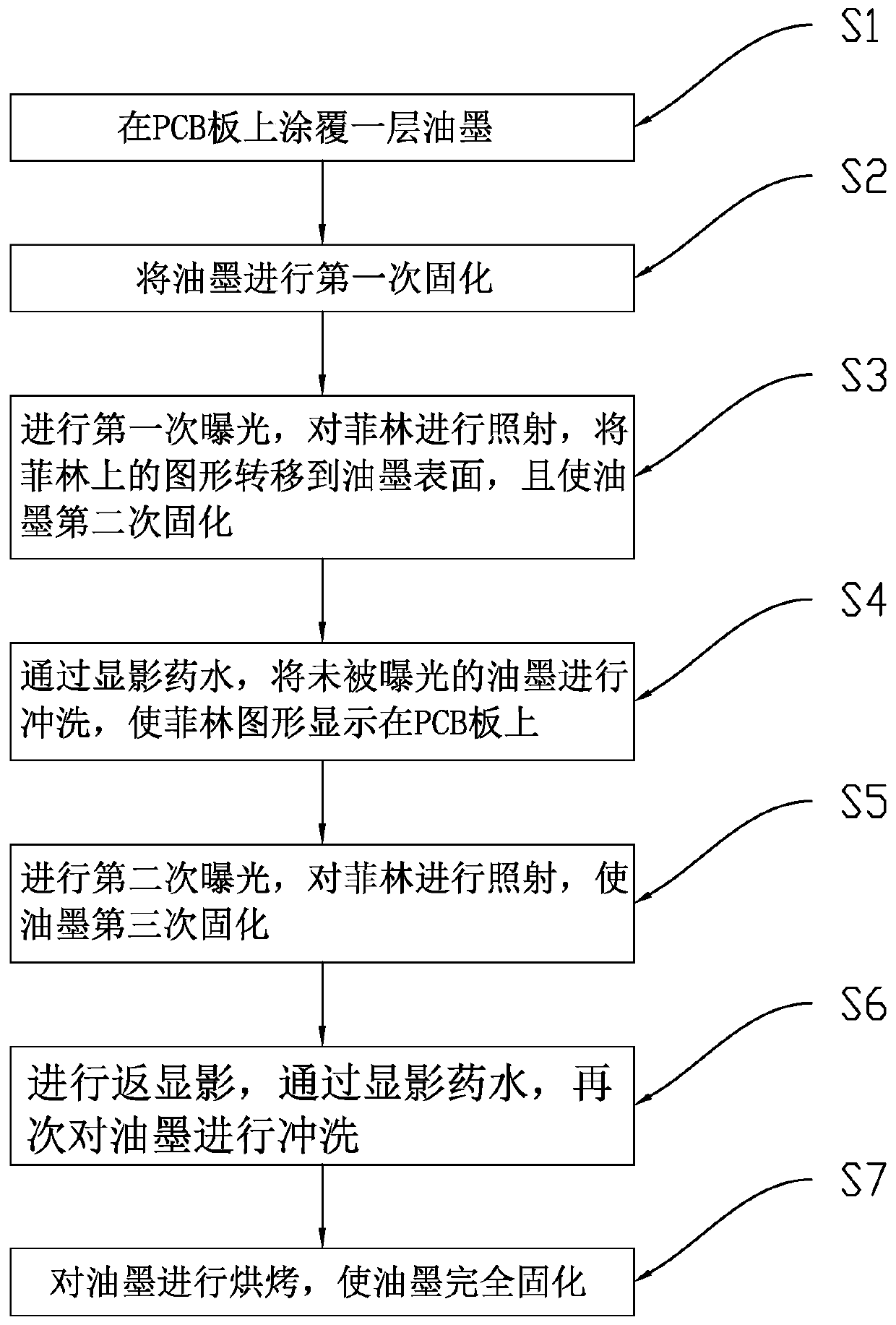
The invention relates to an anti-welding method for small aperture through holes. The method includes the following steps: S1, coating a layer of printing ink on a PCB; S2, performing first curing onthe printing ink; S3, performing first exposure, performing irradiation on a film, transferring a pattern on the film to the surface of the printing ink, and performing second curing on the printing ink; S4, performing washing on unexposed printing ink through a developer so that the film pattern can be displayed on the PCB; S5, performing second exposure, performing irradiation on the film, and performing third curing on the printing ink; S6, performing reverse development, and performing washing on the printing ink again; and S7, performing baking on the printing ink to make the printing inkcompletely cured. Through the first exposure and the second exposure, light curing effects can be increased; reverse development and through holes washing can be performed, so that solder resist bridge and alignment accuracy can be guaranteed to meet quality requirements, the printing ink in holes can be cleaned, risks brought by backwash or repairing can be avoided, and the method is suitable for the making of the through holes with all apertures and spacing.

Description

technical field [0001] The invention relates to the technical field of solder mask through hole processing in PCBs, and more specifically refers to a method for manufacturing through holes with small diameter solder mask holes. Background technique [0002] At present, the production method of solder mask through holes in the PCB industry is generally produced by spraying and dot printing. For holes designed with a window opening of ≤4mil (1mil=25.4μm), the above two methods will cause the problem of ink entering the hole. In addition, the ink hole problem has always been a common problem for solder mask, which affects the first pass rate and has a great quality risk, which cannot meet the production demand. Contents of the invention [0003] The purpose of the present invention is to overcome the defects of the prior art and provide a method for making through holes with small diameter solder resists. [0004] To achieve the above object, the present invention adopts th...

Claims


Application Information

Patent Timeline
Patent Type & Authority Applications(China)
IPC IPC(8): H05K3/28H05K3/22H05K3/26
CPCH05K3/227H05K3/26H05K3/282
Inventor 刘自荣刘芳远王志强
Owner 江西景旺精密电路有限公司
Why Eureka
Try Eureka