Chip detection and packaging production system

A production system and chip detection technology, applied in the field of chip manufacturing, can solve the problems of low detection efficiency, difficult to control and control abnormal quality factors, and leakage, and achieve the effect of stable chip quality, reasonable design and reduced investment.

Pending Publication Date: 2019-11-22
MIANYANG HI TECH ZONE HONGQIANG TECH
View PDF0 Cites 4 Cited by
  • Summary
  • Abstract
  • Description
  • Claims
  • Application Information

AI Technical Summary

Problems solved by technology

Existing inspection, packaging and transfer between them all rely on manual inspection and transfer one by one, the detection efficiency is low, and it is easy to cause leakage, and the abnormal quality factors are difficult to control

Method used


Image

  • Chip detection and packaging production system
  • Chip detection and packaging production system
  • Chip detection and packaging production system

Examples


Embodiment 1

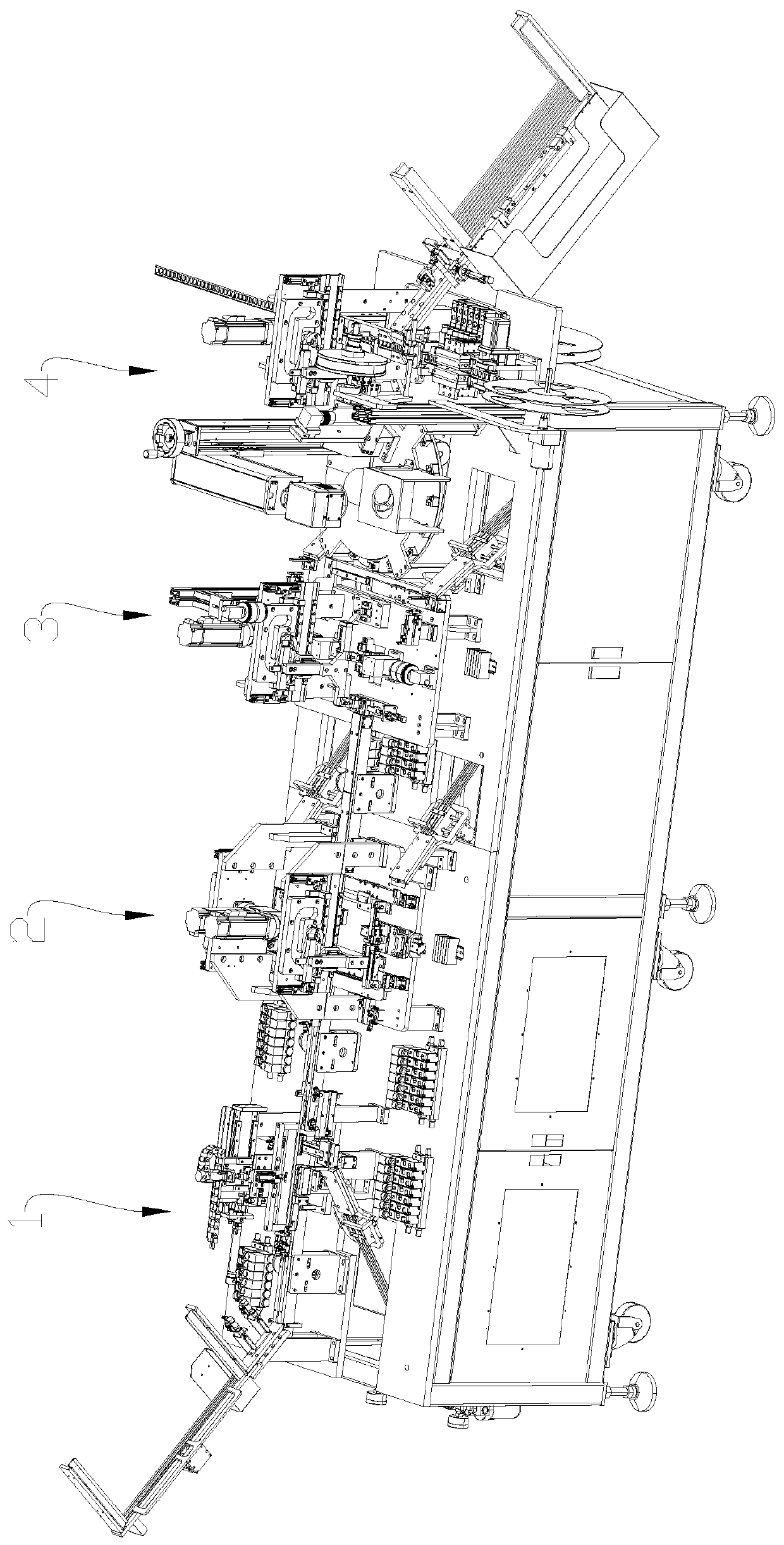
[0029] Such as figure 1 As shown, the present embodiment provides a production system for chip detection and packaging, including a voltage withstand test device 1 for carrying out withstand voltage detection of chips installed on a working platform in sequence, and an electrical test device for carrying out electrical testing of chips. 2, a chip pin foot detection device 3 for testing the flatness, spacing and width of the chip pin feet, and an integrated device 4 for printing and packaging the chip; the first output of the withstand voltage test device 1 The material conveyor belt 16 is connected to the feeding mechanism 221 of the first feeding component 22 of the electrical testing device 2, and the good product transfer mechanism 24 of the electrical testing device 2 is connected to the second feeding component 32 of the chip pin detection device 3, and the chip pin The material transport mechanism 351 of the second defective product collection assembly 35 of the foot det...

Embodiment 2

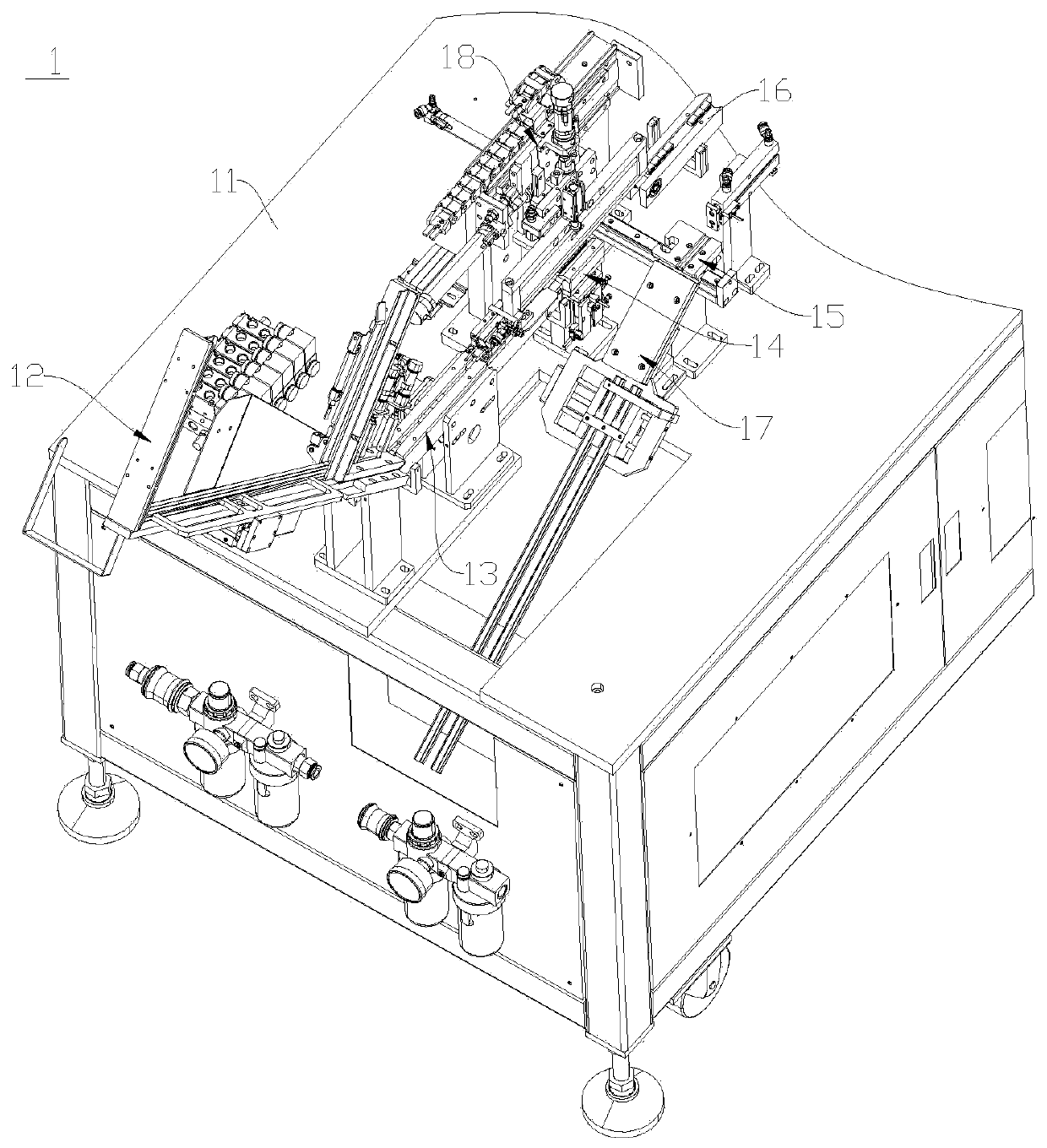
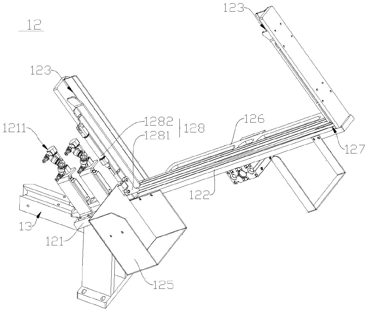
[0031] This embodiment includes all the contents of Embodiment 1, the difference is, as figure 2 As shown, the withstand voltage test device 1 in this embodiment includes a first frame 11 and a blanking mechanism assembly 12 that is sequentially installed on the first frame 11 for blanking, and is used to communicate with the blanking mechanism assembly 12 and transport The feed conveyor belt 13 of the chip, the test fixture 14 for testing the pressure resistance of the chip, the screening mechanism 15 for screening good products and defective products, the first discharge conveyor belt 16 for transporting good products, and the A frame 11 is used to collect the first defective product collection assembly 17 of defective products and the first transfer device used to realize the transfer of chips between the feed conveyor belt 13, the test fixture 14, the screening mechanism 15 and the first discharge conveyor belt 16 Agency18.

[0032] The first frame 11 is installed on the...

Embodiment 3

[0042] This embodiment includes all the content of Embodiment 1, the difference is that in this embodiment, please refer to Figure 11 , The electrical testing device 2 includes a second frame 21 , a first feeding component 22 and a first testing component 23 .

[0043] The second frame 21 is installed on the working platform; the bottom of the second frame 21 is provided with universal wheels to facilitate the transfer of the device, and at the same time in order to ensure the stability of the device in use, the bottom of the second frame 21 is provided with a jacking mechanism , after the working position when moving, the jacking mechanism jacks up the second frame 21, so that the universal wheels are not stressed, and the second frame 21 is not easy to move at this time.

[0044] Such as Figure 16 , Figure 17 As shown, the first feeding assembly 22 includes a feeding mechanism 221 and a first retrieving platform 222. The feeding mechanism 221 is arranged on the second f...


PUM


Abstract

The invention provides a chip detection and packaging production system, and relates to the technical field of chip manufacturing. The chip detection and packaging production system comprises a voltage withstand test device, an electrical test device, a chip pin detection device and an integrated device which are sequentially installed on a working platform, wherein the voltage withstand test device is used for carrying out voltage withstand detection on a chip; the electrical test device is used for carrying out electrical detection on the chip; the chip pin detection device is used for detecting the flatness, the intervals and the widths of chip pins; the integrated device is used for printing and packaging the chip; a first discharging conveyer belt of the voltage withstand test devicecommunicates with a feeding mechanism of a first feeding assembly of the electrical test device; a good product transferring mechanism of the electrical test device communicates with a second feedingassembly of the chip pin detection device; and a conveying mechanism of a second defective product collecting assembly of the chip pin detection device communicates with a conveying device of a printing assembly of the integrated device. According to the chip detection and packaging production system, the design is reasonable, the chip can be detected automatically and continuously, the labor investment is reduced, the detection omissions are avoided, and the chip quality is stable.

Description

technical field [0001] The invention relates to the technical field of chip manufacturing, in particular to a chip detection and packaging production system. Background technique [0002] SMD (abbreviation for Surface Mounted Devices), that is, surface mount devices, mainly includes rectangular chip materials, cylindrical chip materials, composite chip materials, and special-shaped chip materials. For rectangular chip surface mount devices, it is necessary to test the specifications and parameters of the finished product after the production is completed. After passing the test, the product is packaged by packaging equipment such as a packaging machine, that is, the production of the entire electronic product is completed. Existing inspection, packaging, and transfer between them all rely on manual inspection and transfer one by one. The detection efficiency is low, and it is easy to cause leakage, and it is difficult to control abnormal quality factors. Contents of the in...

Claims


Application Information

Patent Timeline
Patent Type & Authority Applications(China)
IPC IPC(8): B07C5/344B07C5/34B07C5/36B07C5/38B07C5/02B07C5/04
CPCB07C5/02B07C5/04B07C5/34B07C5/344B07C5/362B07C5/38
Inventor 豆宏春刘军王强
Owner MIANYANG HI TECH ZONE HONGQIANG TECH
Why Eureka
Try Eureka