A voltage clamping circuit and buck converter
A voltage clamping and circuit technology, applied in the direction of output power conversion devices, instruments, electrical components, etc., can solve problems such as complex circuit structures, achieve the effects of simplifying circuit difficulty, saving chip area, and solving complex circuit structures
- Summary
- Abstract
- Description
- Claims
- Application Information
AI Technical Summary
Problems solved by technology
Method used
Image
Examples
Embodiment approach
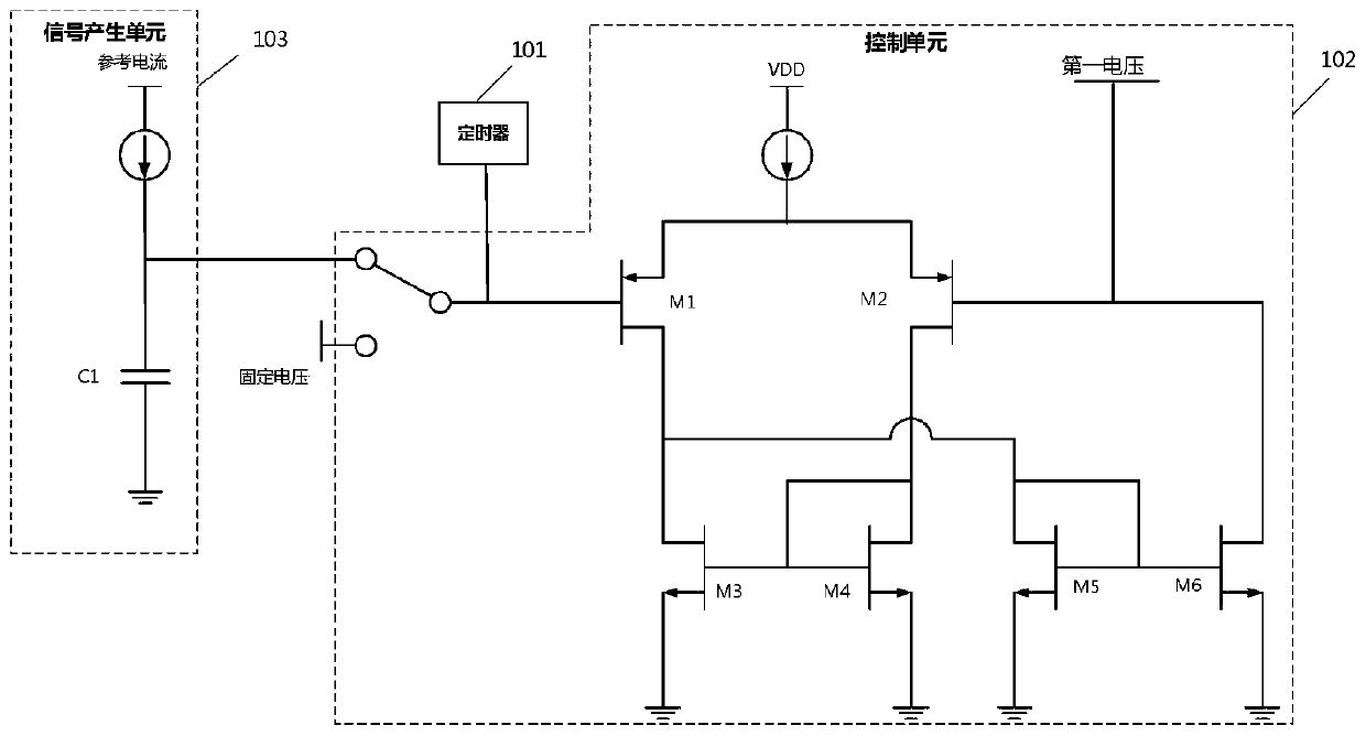
[0064] See figure 2 , in another specific embodiment of the present application, an implementation manner of the signal generating unit 103 includes: a first capacitor C1.
[0065] Wherein, the first terminal of the first capacitor C1 receives the reference current, and the second terminal is grounded. The first end of the first capacitor C1 receiving the reference current is used as the output end of the signal generating unit.
[0066] In practical application, the voltage change in the reference current can be seen from image 3 , is the voltage gradually increasing from 0 to the working voltage VDD, that is, the incremental signal generated by the signal generating unit 103 .
[0067] Of course, the magnitude and change mode of the voltage of the reference current can also be set according to the application environment and user needs, which are not specifically limited in this application, and all belong to the protection scope of this application.
[0068] see also ...
specific Embodiment approach
[0113] Optionally, see also Figure 5 , in a specific embodiment of the present application, a specific implementation manner of the filtering unit 406 includes:
[0114] The first inductor L and the third capacitor C3.
[0115] A first end of the first inductor L is connected to the drain of the PMOS transistor, and a second end of the third capacitor C3 is grounded. Wherein, the common terminal of the first inductor L and the third capacitor C3 is used as the output terminal of the filter unit 406 to output the output voltage.
[0116] It should be noted that the third voltage can be filtered through the first inductor L and the third capacitor C3, which can reduce the ripple of the output voltage output by the step-down converter.
PUM
 Abstract
Description
Claims
Application Information


