
Fan-out chip packaging structure and packaging method

A chip packaging structure and chip packaging technology, applied in the direction of electrical components, electric solid devices, circuits, etc., can solve the problems of low reliability of packaging structure, stress fracture failure, etc. , the effect of improving reliability

Active Publication Date: 2019-11-29
江苏中科智芯集成科技有限公司
View PDF5 Cites 2 Cited by
  • Summary
  • Abstract
  • Description
  • Claims
  • Application Information

AI Technical Summary

Problems solved by technology

[0004] Therefore, the technical problem to be solved by the present invention is to solve the problem that the rewiring in the existing packaging structure is prone to failure due to stress fracture when the expansion coefficients of the chip and the plastic packaging material do not match, and the reliability of the packaging structure is low.

Method used


Image

  • Fan-out chip packaging structure and packaging method
  • Fan-out chip packaging structure and packaging method
  • Fan-out chip packaging structure and packaging method

Examples


Embodiment 1

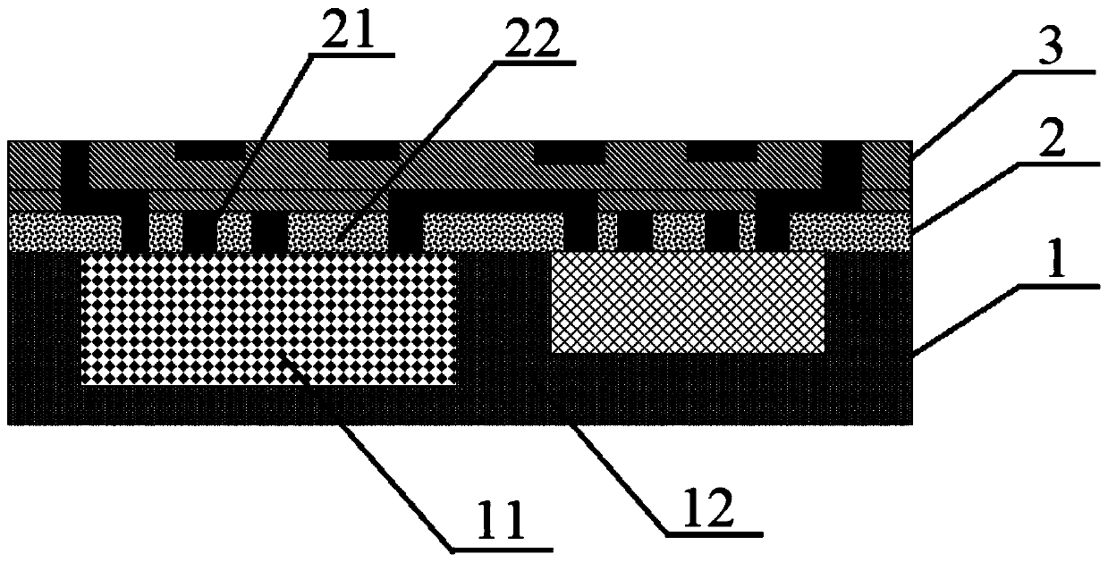
[0030] This embodiment provides a fan-out chip packaging structure, such as figure 1 As shown, the packaging structure includes: a plastic package body 1 , an interconnection layer 2 and a redistribution layer 3 .

[0031] Such as figure 1 As shown, at least one chip 11 is packaged inside the plastic package 1 , and the device surface of the chip 11 is exposed outside the plastic package 1 . Here, the device surface of the chip 11 refers to the surface where the pads of the chip 11 are located. Specifically, the chip 11 can be first mounted on the substrate 4 according to the direction that the device surface of the chip 11 faces the substrate 4, and then mounted on the substrate 4. The molding compound is injected to form the molding layer 12 that encapsulates five surfaces of the chip 11 except the device surface, and then the molding layer 12 and the chip 11 are peeled off from the substrate 4 to form the molding body 1 .

[0032] Such as figure 1 As shown, the interconn...

Embodiment 2

[0040] This embodiment provides a fan-out chip packaging method, and the packaging structure in Embodiment 1 can be prepared according to the method and its preferred implementation, and what has been explained will not be repeated.

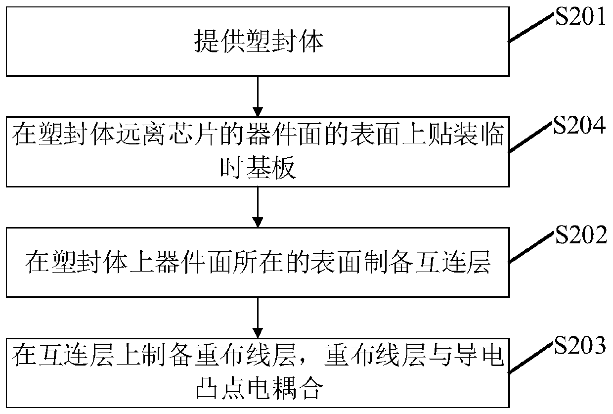
[0041] The fan-out chip packaging method provided in this embodiment, such as figure 2 shown, including the following steps:

[0042] S201: Provide a plastic package.

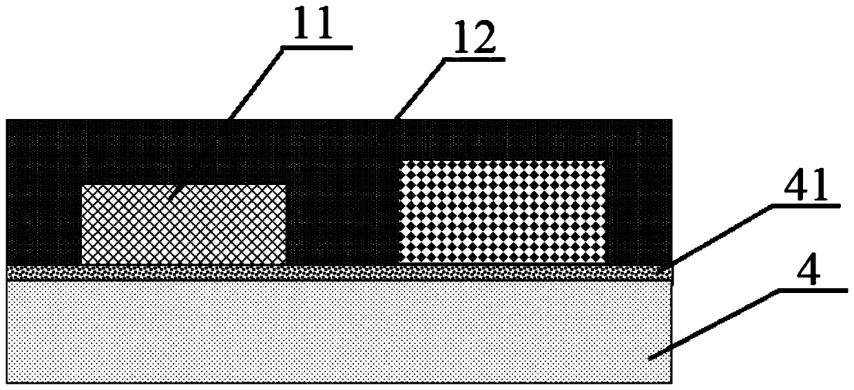
[0043] here, as image 3 As shown, at least one chip 11 is packaged inside the plastic package 1 , and the device surface of the chip 11 is exposed outside the plastic package 1 .

[0044] Specifically, such as image 3 As shown, the plastic package 1 can be prepared by the following steps:

[0045] Step A1: pasting a first temporary bonding glue 41 on a substrate 4 .

[0046] Step A2: paste the chip 11 on the first temporary bonding glue 41 according to the direction that the device surface of the chip 11 faces the first temporary bonding glue 41 .

[0047] Step A3: dispos...


PUM


Abstract

The invention discloses a fan-out chip packaging structure and a packaging method. The packaging structure comprises a plastic packaging body, an interconnection layer and a rewiring layer, wherein the plastic packaging body is internally packaged with at least one chip, and the device surface of the chip is exposed out of the plastic packaging body; the interconnection layer is arranged on the surface of the device surface of the plastic packaging body and is internally provided with a conductive convex point corresponding to a pad of the chip, and the conductive convex point is used for leading out the corresponding pad to the upper surface of the interconnection layer; and the rewiring layer is arranged on the interconnection layer, and the rewiring layer is electrically coupled with the convex point. As the interconnection layer is arranged between the rewiring layer and the plastic packaging body, the interface stress between the plastic packaging body and the chip is greatly reduced after passing through the interconnection layer, the stress borne by the rewiring layer can be greatly reduced, the possibility of fatigue fracture due to the influence of the interface stress onthin and narrow rewiring is greatly reduced, and the reliability of the packaging structure is improved.

Description

technical field [0001] The invention relates to the technical field of semiconductor integrated circuit packaging, in particular to a fan-out chip packaging structure and packaging method. Background technique [0002] As the most cost-effective technology in the field of system integration packaging, wafer-level fan-out packaging technology will gradually lead the development direction of future system integration technology by virtue of its advantages of high density, light weight and short size, good heat dissipation performance and good electrical performance. . At present, fan-out packaging technology is developing towards next-generation packaging technologies such as multi-chip, thin packaging and three-dimensional system integration. [0003] However, there are still many problems to be solved in fan-out packaging technology, among which the reliability of multi-chip integrated rewiring is one of the problems. Specifically, due to the large difference in thermal ex...

Claims


Application Information

Patent Timeline
Patent Type & Authority Applications(China)
IPC IPC(8): H01L23/31H01L23/485H01L23/488H01L21/56H01L21/60
CPCH01L23/3107H01L23/485H01L24/02H01L24/03H01L21/568H01L2224/0231H01L2224/0233H01L2224/02373H01L2224/02379H01L2224/18H01L2224/24137H01L2224/96H01L2924/3511
Inventor 姚大平
Owner 江苏中科智芯集成科技有限公司
Learn More